Transcription of Metal/Semiconductor Ohmic Contacts - Stanford University
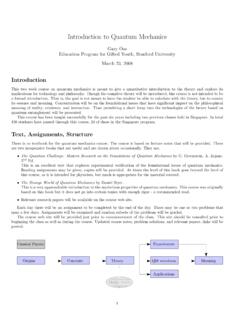
1 EE311 notes/ SaraswatMetal/Semiconductor Ohmic ContactsRcsdRdpRextRovxy = 0 GateSidewallSilicideNext(x)Nov(y)Year199 719992003200620092012 Min Feature Contact xj (nm)100-20070-14050-10040-8015-3010-20xj at Channel (nm) components of the resistance associated with the S/D junctions of a MOS will be a dominant component for highly scaled nanometer transistor (Rcsd/Rseries >> ~ 60 % for LG < 53 nm)32 nm53 nm70 nm100 nm010203040506070 RdpRextRovRcsdNMOSP hysical Gate Length Relative Contribution [%] 30 nm50 nm70 nm100 nm020406080100120140 NMOSS caled by ITRS Roadmap RcsdRdpRextRovTechnology or Gate LengthSeries Resistance (ohms)EE311 / Saraswat Ohmic Contacts232 nm53 nm70 nm100 nm010203040506070 Physical Gate LengthRdpRovRextRcsdPMOS Relative Contribution [%] 30 nm50 nm70 nm100 nm050100150200 PMOSS caled by ITRS RoadmapRcsdRdpRextRov Technology or Gate LengthSeries Resistance (ohms)Fig.
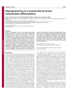
2 2. Various components of the resistance associated with the shallow junctions ofNMOS and PMOS transistors for different technology nodes. (Source: Jason Woo,UCLA)Conduction Mechanisms for Metal/Semiconductor ContactsEfVIOhmicSchottky(c) Field emission. (a) Thermionic emission (b) Thermionic-field emissionLow dopingMedium dopingHeavy dopingFig. 3. Conduction mechanisms for metal/n-semiconductor Contacts as a function of thebarrier height and width. (a) Thermionic emission; (b) thermionic-field emission; (c) / Saraswat Ohmic Contacts3(1)Thermionic emission (TE), occurring in the case of a depletion region so wide that theonly way for electrons to jump the potential barrier is by emission over its maximum ( ).
3 The barrier height is reduced from its original value as a result of image force barrierlowering.(2)Field emission (FE), consisting in carrier tunneling through the potential barrier. Thismechanism, which is the preferred transport mode in Ohmic Contacts , takes place when thedepletion layer is sufficiently narrow, as a consequence of the high doping concentration inthe semiconductor (Fig. 3c).Contact Resistance and Specific Contact Resistivity ( c)Contact resistance is a measure of the ease with which current can flow across a metal-semiconductor interface.
4 In an Ohmic interface, the total current density J entering the interfaceis a function of the difference in the equilibrium Fermi levels on the two band diagram in the Fig. 4 may be used as an aid in describing the majority current flowin the block of uniformly heavily doped semiconductor material of length l with ohmiccontacts at each end. The applied voltage V drives a spatially uniform current I through thesemiconductor bulk and Ohmic Contacts of cross sectional area A. Then, under the low-currentassumption that the voltage drop across both metal-semiconductor Contacts is identical, theI-V relation becomes: V Vn+Figure 4.
5 Ideal Contacts to a heavily doped semiconductor with uniform current = Vbulk + 2 Vcontact = (Rbulk + 2 Rcontact)I =(1)Rbulk=dVbulkdI= lARcontact=dVcontactdI= cA(2)where is the bulk resistivity and c specific contact resistivity that can be defined throughthe component the voltage required to drive current through a good Ohmic contact is small we restrictthe c definition to zero applied voltage. c=V 0limdVcontactdJ cm2(3)EE311 / Saraswat Ohmic Contacts4where J is the current density I/A. Alternatively (3) can be defined asJ=vmetal vsemicond c(3a)Thermionic Emission - Schottky ContactFor a Schottky contact the current governed by thermionic emission over the barrier is givenby JS=A*T2exp 2 BkT eqVkT 1()(4)where A* is Richardson s constant.
6 The specific contact resistivity as calculated by Eq. (3)is c=kqA*Texp2 BkT =kTqJs(5)Tunneling - Ohmic ContactsAn Ohmic contact is defined as one in which there is an unimpeded transfer of majoritycarriers from one material to another, , the Contacts do not limit the current. The way toachieve such a contact is by doping the semiconductor heavily enough that tunneling ispossible. It is usual to heavily dope the Si regions N+ or P+ so that an Ohmic contact isinsured. Suppose Nd (or Na) in the semiconductor is very large.
7 Then the depletion regionwidth at the metal - semiconductor interfaceXd=2K o iqNd becomes very small. When Xd < 5nm, electrons can tunnel through the process occurs in both directions M S and S M so the contact shows very littleresistance and becomes calculate an approximate value for the required doping, Ndmin 2K o iqXd2 1019cm 3for Xd= is a relatively easy value to achieve in practice and is normally how Ohmic Contacts aremade in integrated circuits. EE311 / Saraswat Ohmic Contacts5 For a tunneling contact the net semiconductor to metal current is given byJsm=A*TkFs P(E)(1 Fm)dE(6)where Fs and Fm are Fermi-Dirac distribution functions in metal and semiconductorrespectively, and P(E) is the tunneling probability given by P(E)~exp-2 Bh sm*N (7)Where m* is the effective mass of the tunneling carrier and h is the Plank's constant.
8 Theanalysis to calculate current is more is somewhat more complicated, resulting in Jsm exp 2xd2m*q B qV()/h2[]Specific contact resistivity can be calculated using equations described above and is of theform c= coexp2 Bh sm*N ohm cm2(8)Where co is a constant dependent upon metal and the semiconductor. Specific contactresistivity, c primarily depends upon the metal-semiconductor work function, , doping density, N, in the semiconductor and the effective mass of the carrier, m*.EE311 / Saraswat Ohmic Contacts6 Fig.
9 5. Specific contact resistivity of metal Contacts to n-type and p-type Si. Solid lines arecalculated from the model. (Ref: S. Swirhun, Electrochem. Soc., Oct. 1988)Observations1. Specific contact resistivity, c as barrier height 3. For a given doping density contact resistance is higher for n-type Si than can be attributed to the barrier height2. Specific contact resistivity, c as doping density Doping density can t be scaled beyond solid solubility. N type dopants have higher solid solubility than P type dopantsEE311 / Saraswat Ohmic Contacts7 Fig.
10 8. Solid solubility of dopants in Si (Ref: Plummer & Griffin, Proc. IEEE, April 2001)Barrier HeightFigure: 9 Accumulation and depletion type is the physical parameter that describes the transport of majority carriers across heavilydoped Si-metal interfaces. However, experiment and modeling of Ohmic conduction is stillcrude. An Ohmic contact is generally modeled as a heavily doped Schottky (diode) Schottky model predicts that upon bringing in contact Si with electron affinity X, and ametal of work function m, a barrier of height b= m () which is independent ofsemiconductor doping will be formed.