Transcription of Metal/Semiconductor Ohmic Contacts - Stanford University
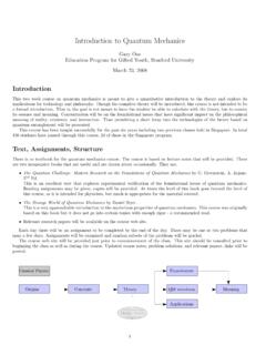
1 EE311 notes/ SaraswatMetal/Semiconductor Ohmic ContactsRcsdRdpRextRovxy = 0 GateSidewallSilicideNext(x)Nov(y)Year199 719992003200620092012 Min Feature Contact xj (nm)100-20070-14050-10040-8015-3010-20xj at Channel (nm) components of the resistance associated with the S/D junctions of a MOS will be a dominant component for highly scaled nanometer transistor (Rcsd/Rseries >> ~ 60 % for LG < 53 nm)32 nm53 nm70 nm100 nm010203040506070 RdpRextRovRcsdNMOSP hysical Gate Length Relative Contribution [%] 30 nm50 nm70 nm100 nm020406080100120140 NMOSS caled by ITRS Roadmap RcsdRdpRextRovTechnology or Gate LengthSeries Resistance (ohms)EE311 / Saraswat Ohmic Contacts232 nm53 nm70 nm100 nm010203040506070 Physical Gate LengthRdpRovRextRcsdPMOS Relative Contribution [%] 30 nm50 nm70 nm100 nm050100150200 PMOSS caled by ITRS RoadmapRcsdRdpRextRov Technology or Gate LengthSeries Resistance (ohms)Fig.
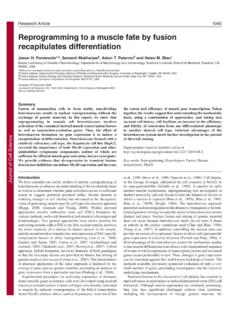
2 2. Various components of the resistance associated with the shallow junctions ofNMOS and PMOS transistors for different technology nodes. (Source: Jason Woo,UCLA)Conduction Mechanisms for Metal/Semiconductor ContactsEfVIOhmicSchottky(c) Field emission. (a) Thermionic emission (b) Thermionic-field emissionLow dopingMedium dopingHeavy dopingFig. 3. Conduction mechanisms for metal/n-semiconductor Contacts as a function of thebarrier height and width. (a) Thermionic emission; (b) thermionic-field emission; (c) / Saraswat Ohmic Contacts3(1)Thermionic emission (TE), occurring in the case of a depletion region so wide that theonly way for electrons to jump the potential barrier is by emission over its maximum ( ). The barrier height is reduced from its original value as a result of image force barrierlowering.(2)Field emission (FE), consisting in carrier tunneling through the potential barrier.
3 Thismechanism, which is the preferred transport mode in Ohmic Contacts , takes place when thedepletion layer is sufficiently narrow, as a consequence of the high doping concentration inthe semiconductor (Fig. 3c).Contact Resistance and specific Contact Resistivity ( c)Contact resistance is a measure of the ease with which current can flow across a metal-semiconductor interface. In an Ohmic interface, the total current density J entering the interfaceis a function of the difference in the equilibrium Fermi levels on the two band diagram in the Fig. 4 may be used as an aid in describing the majority current flowin the block of uniformly heavily doped semiconductor material of length l with ohmiccontacts at each end. The applied voltage V drives a spatially uniform current I through thesemiconductor bulk and Ohmic Contacts of cross sectional area A. Then, under the low-currentassumption that the voltage drop across both metal-semiconductor Contacts is identical, theI-V relation becomes: V Vn+Figure 4: Ideal Contacts to a heavily doped semiconductor with uniform current = Vbulk + 2 Vcontact = (Rbulk + 2 Rcontact)I =(1)Rbulk=dVbulkdI= lARcontact=dVcontactdI= cA(2)where is the bulk resistivity and c specific contact resistivity that can be defined throughthe component the voltage required to drive current through a good Ohmic contact is small we restrictthe c definition to zero applied voltage.
4 C=V 0limdVcontactdJ cm2(3)EE311 / Saraswat Ohmic Contacts4where J is the current density I/A. Alternatively (3) can be defined asJ=vmetal vsemicond c(3a)Thermionic Emission - Schottky ContactFor a Schottky contact the current governed by thermionic emission over the barrier is givenby JS=A*T2exp 2 BkT eqVkT 1()(4)where A* is Richardson s constant. The specific contact resistivity as calculated by Eq. (3)is c=kqA*Texp2 BkT =kTqJs(5)Tunneling - Ohmic ContactsAn Ohmic contact is defined as one in which there is an unimpeded transfer of majoritycarriers from one material to another, , the Contacts do not limit the current. The way toachieve such a contact is by doping the semiconductor heavily enough that tunneling ispossible. It is usual to heavily dope the Si regions N+ or P+ so that an Ohmic contact isinsured.
5 Suppose Nd (or Na) in the semiconductor is very large. Then the depletion regionwidth at the metal - semiconductor interfaceXd=2K o iqNd becomes very small. When Xd < 5nm, electrons can tunnel through the process occurs in both directions M S and S M so the contact shows very littleresistance and becomes calculate an approximate value for the required doping, Ndmin 2K o iqXd2 1019cm 3for Xd= is a relatively easy value to achieve in practice and is normally how Ohmic Contacts aremade in integrated circuits. EE311 / Saraswat Ohmic Contacts5 For a tunneling contact the net semiconductor to metal current is given byJsm=A*TkFs P(E)(1 Fm)dE(6)where Fs and Fm are Fermi-Dirac distribution functions in metal and semiconductorrespectively, and P(E) is the tunneling probability given by P(E)~exp-2 Bh sm*N (7)Where m* is the effective mass of the tunneling carrier and h is the Plank's constant.
6 Theanalysis to calculate current is more is somewhat more complicated, resulting in Jsm exp 2xd2m*q B qV()/h2[] specific contact resistivity can be calculated using equations described above and is of theform c= coexp2 Bh sm*N ohm cm2(8)Where co is a constant dependent upon metal and the semiconductor. specific contactresistivity, c primarily depends upon the metal-semiconductor work function, , doping density, N, in the semiconductor and the effective mass of the carrier, m*.EE311 / Saraswat Ohmic Contacts6 Fig. 5. specific contact resistivity of metal Contacts to n-type and p-type Si. Solid lines arecalculated from the model. (Ref: S. Swirhun, Electrochem. Soc., Oct. 1988)Observations1. specific contact resistivity, c as barrier height 3. For a given doping density contact resistance is higher for n-type Si than can be attributed to the barrier height2.
7 specific contact resistivity, c as doping density Doping density can t be scaled beyond solid solubility. N type dopants have higher solid solubility than P type dopantsEE311 / Saraswat Ohmic Contacts7 Fig. 8. Solid solubility of dopants in Si (Ref: Plummer & Griffin, Proc. IEEE, April 2001)Barrier HeightFigure: 9 Accumulation and depletion type is the physical parameter that describes the transport of majority carriers across heavilydoped Si-metal interfaces. However, experiment and modeling of Ohmic conduction is stillcrude. An Ohmic contact is generally modeled as a heavily doped Schottky (diode) Schottky model predicts that upon bringing in contact Si with electron affinity X, and ametal of work function m, a barrier of height b= m () which is independent ofsemiconductor doping will be formed. Since measured m values for a variety of metalsrange from about to eV, and Si eV, this model should predict bothaccumulation and depletion (Fig.)
8 9) metal-semiconductor Contacts . This is generally notseen with Si; there is little evidence for the existence of any accumulation type metal toheavily doped Si contact. The reason is poorly understood but related to the restructuringof the metal-silicon surface. All practical n and p type Ohmic Contacts to Si are barrier heights that are used in modeling Ohmic contact to Si are empirical values,EE311 / Saraswat Ohmic Contacts8usually measured by capacitance-voltage, current-voltage or photoemission and silicide barrier heights to both n and p type Si as a function of metal work functionare illustrated in Fig. 10. The thin vertical lines connect data points for the same metal. Thestronger b dependence of metallic suicides on m has led to the postulation that someinterface cleanliness or the presence of an interfacial layer affects barrier height.
9 Silicides areknown to make more intimate contact to 10: Metal-semiconductor barrier height to n- and p-type Si ( bn - hollow symbols and bpsolid symbols) vs. metal work function. (Ref: S. Swirhun, PhD Thesis, Stanford Univ. 1987)It can be noticed that the Fermi level pinning is roughly at the same energy within theforbidden gap for both n and p type Si ( the sum of bn and bp, is approximately Egsuggesting that interface and structural factors pin the Fermi level because of a very highdensity of interface states (Fig. 11). Note that for Ohmic Contacts we never need worryabout the occupancy of these states changing, because of very small potential drop acrossthe contact. BN + BP = EgFigure. 11 Metal-semiconductor barrier height to n-type and p-type SiEE311 / Saraswat Ohmic Contacts9 Strategy for Series Resistance Scaling0306090120150180210240270300 RcsdRdpRextRovSource/Drain EngineeringBox ProfileLow-BarrierSilicide( B = eV)Box ProfileMidgap SilicideGraded JunctionMidgap Silicide LG = 53 nmS/D Series Resistance [ m]Source: Jason Woo, (UCLA)RcsdRdpRextRovxy = 0 GateSidewallSilicideNext(x)Nov(y) Rdp & Rcsd Scaling ( c ) Maximize Nif ( Rsh,dp ):- Laser annealing- Elevated S/D Minimize B:- Dual low-barrier silicide (ErSi (PtSi2) for N(P)MOS) Rov & Rext Scaling Dopant Profile Control: ultra-shallow highly-doped box-shaped SDE profile ( , laser annealing, PAI + Laser Annealing)EE311 / Saraswat Ohmic Contacts10 Bandgap EngineeringContact resistance depends on barrier height.)
10 It is possible to use a lower bandgapmaterial in the source/drain such as Si1-xGex. Band gap of Si1-xGex reduces ascompared to Si as Ge fraction increases. Si1-xGex S/D & germanosilicide contact Assuming metal Fermi level is pinned near midgap Similar barrier heights on n- or p-type material Smaller bandgap for Si1-xGex Reduction of Rcsd with single contact metalFrom M. C. Ozturk et al. (NCSU), IEDM2002EE311 / Saraswat Ohmic Contacts11 Accurate Modeling of Contact ResistanceIn practice it is difficult to construct a practical sized contact that passes a uniform currentdensity over its area so this definition is usually considered in the limit as the elementalcontact area approaches a uniform current density c can be defined as contact resistance per unit the situation becomes complicated in real device structures as the currentdistribution is non-uniform.