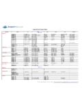
Transcription of Micro SD Data Sheet - Super Talent Technology
1 Micro SDSC / SDHC / SDXC. Micro SD Data Sheet Rev. 1 APR 2012. Micro SDSC / SDHC / SDXC. Table of Contents 1. Introduction to the Micro SDSC/SDHC/SDXC .. 4. 2. Micro SDSC/SDHC/SDXC Feature .. 4. 3. Product .. 6. 4. Micro S SDSC/SDHC/SDXC Interface Description .. 7. 5. Mechanical Form Factor ..15. Rev. 2 APR 2012. Micro SDSC / SDHC / SDXC. Revision History Date Revision History APR 2012 New Creation Rev. 3 APR 2012. Micro SDSC / SDHC / SDXC. 1. Introduction to the Micro SDSC/SDHC/SDXC. Micro SD Card is a Flash Based memory card that is designed to meet the security, capacity, performance and environment requirements inherent to use in emerging audio and video electronic device. The Micro SD Card communication is based on an advance 8-pin interface (clock, command, 4x Data and 2x power lines) and the Micro SD Memory Card host interface supports regular Multi Media Card operation as well.
2 2. System Features Targeted for portable and stationary applications Capacity of Memory (1) Standard Capacity SD Memory card (SDSC): Up to and including 2 GB. (2) High Capacity SD Memory Card (SDHC): More than 2GB and up to and including 32GB. (3) Extended Capacity SD Memory Card (SDXC): More than 32GB and up to and including 2TB. Voltage range: High Voltage SD Memory Card Operating voltage range: V. Designed for read-only and read/write cards. Compliant SD Card Specification ver. Bus Speed Mode (using 4 parallel data lines). (1) Default Speed mode: signaling, Frequency up to 25 MHz, up to MB/sec (2) High Speed mode: signaling, Frequency up to 50 MHz, up to 25 MB/sec (3) SDR12: signaling, Frequency up to 25 MHz, up to (4) SDR25: signaling, Frequency up to 50 MHz, up to 25MB/sec (5) SDR50: signaling, Frequency up to 100 MHz, up to 50MB/sec (6) SDR104: signaling, Frequency up to 208 MHz, up to 104MB/sec (7) DDR50: signaling, Frequency up to 50 MHz, sampled on both clock edges, up to 50MB/sec Switch function command supports High-Speed, and future functions Correction of memory field errors Card removal during read operation will never harm the content Content Protection Mechanism - Complies with highest security of SDMI standard.
3 Password Protection of cards (CMD42 - LOCK_UNLOCK). Write Protect feature using mechanical switch Built-in write protection features (permanent and temporary). Card Detection (Insertion/Removal). Application specific commands Comfortable erase mechanism Rev. 4 APR 2012. Micro SDSC / SDHC / SDXC. System Block Diagram Speed Class Five Speed Classes are defined and indicate minimum performance of the cards Class 0 - These class cards do not specify performance. It includes all the legacy cards prior to this specification, regardless of its performance Class 2 is more than or equal to 2 MB/sec performance Class 4 is more than or equal to 4 MB/sec performance Class 6 is more than or equal to 6 MB/sec performance Class 10 is more than or equal to 10 MB/sec performance Dimension: x Support CPRM. No external programming voltage required SD Memory Card protocol compatible Targeted for portable and stationary applications for secured (copyrights protected) and non-secured data storage Correction of memory field errors Copyrights Protection Mechanism: Complies with highest security of SDMI standard Card Detection (Insertion / Removal).
4 CE and FCC certificates Easy handling for the end user Notes: The performance depends on different test platform with different result. The communication channel is described in the table below Micro SDSC/SDHC/SDXC Bus/SPI Bus comparison Micro SDSC/SDHC/SDXC Using SD Bus Micro SDSC/SDHC/SDXC Using SPI Bus Six-wire communication channel Three-wire serial data bus (Clock, dataIn, data Out )+card (clock, command, 4 data lines) specific CS signal(hardwired card selection). Error-protected data transfer Optional non protected data transfer mode available Single or multiple block oriented data transfer Single or multiple block oriented data transfer Rev. 5 APR 2012. Micro SDSC / SDHC / SDXC. 3. Product Specification Reliability and Durability Specifications to 85 . Operating: -25. Storage: -40 (168h) to 85 (500h).
5 Temperature Operating: 25 C / 95% rel. humidity Non-Operating: 40 C / 93% rel. moisture and corrosion salt water spray: 3% NaCl/35C; 24h acc. MIL STD Method 1009. Durability 10,000 mating cycles Bending 10N. Torque *m. max Drop Test free fall No warp age; no mold slim; complete form; no cavities; surface Visual Inspection/Shape and Form smoothness cm2 within contour; no cracks; no pollution (oil, dust, etc.). System Reliability and Maintenance MTBF >1,000,000 hours Preventive Maintenance None Data Reliability < 1 non-recoverable error in 1014 bits read Endurance MLC 3,000~10,000 write/erase cycles TLC 500~1,000 write/erase cycles Electrical Static Discharge (ESD) requirement Contact Discharge: 4KV, Human body model according to ESD Protection 8KV, Human body model according to Air Discharge; Rev.
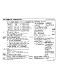
6 6 APR 2012. Micro SDSC / SDHC / SDXC. 4. Micro SDSC/SDHC/SCXC Interface Description General Description of Pins and Registers The Micro SDHC has nine exposed contacts on one side. The host is connected to the SD Memory Card using a eight pin connector. Pin Assignment in SD Bus Mode Pad Definition Pin # Name Type Micro SD Description 1 DAT2 I/O Card Detect/ Data Lin [Bit 3]. 2 CD/DAT3 I/O Card Detect / Data Line 3 CMD PP Command / Response 4 VDD S Supply voltage 5 CLK I Clock 6 Vss S Supply voltage ground 7 DAT0 I/O Data Line [Bit 0]. 8 DAT1 I/O Data Line [Bit 1]. Note: 1) S=power supply; I=input; O=output using push-pull drivers. 2) The extended DAT lines (DAT1-DAT3) are input on power up; they start to operate as DAT lines after the SET _BUS_WIDTH command. 3) After power up, this line is input with 50 Kohm pull-up (can be used for card detection or SPI mode selection).
7 The pull-up should be disconnected by the user, during regular data transfer, with SET_CLR_CARD_DETECT. (ACMD42) command. Pin Assignment in SPI Bus Mode Pad Definition Pin # Name Type Micro SD Description 1 RSV Reserved 2 CS I Chip Select (neg true). 3 DI S Data In 4 VDD S Supply Voltage 5 SCLK I Clock 6 VSS S Supply Voltage Ground 7 DO O Data Out 8 RSV I Reserved Each card has a set of information registers Micro SD Memory Card Registers Name Width Description CID 128 Card identification number: individual card number for identification. Relative card address: local system address of a card dynamically RCA 16. suggested by the card and approved by the host during initialization CSD 128 Card specific data: information about the card operation conditions. SD Configuration Register: information about the Micro SD Card's special SCR 64.
8 Feature capabilities. OCR 32 Operation Condition Register The host may reset the cards by switching the power supply off and on again. The card has its own power-on detection circuitry which puts the card into an idle state after the power-on. The card can also be reset by sending the GO_IDLE (CMD0) command. Rev. 7 APR 2012. Micro SDSC / SDHC / SDXC. Micro SD memory Card Pin Assignment Micro SD memory Card contact Area SD Bus Topology The SD bus has six communication lines and three supply lines: CMD: Command is bi-directional signal.(Host and card drivers are operating in push pull mode.). DAT0-3: Data lines are bi-directional signals. (Host and card drivers are operating in push pull mode.). CLK: Clock is a host to cards signal. (CLK operates in push pull mode.). VDD: VDD is the power supply line for all cards.
9 VSS [1:2]: VSS are two ground lines. The following figure shows the bus topology of several cards with one host in SD Bus mode. Micro SD Memory Card System Bus Topology Rev. 8 APR 2012. Micro SDSC / SDHC / SDXC. During the initialization process, commands are sent to each card individually, allowing the application to detect the cards and assign logical addresses to the physical slots. Data is always sent to each card individually. However, to simplify the handling of the card stack, after initialization, all commands may be sent concurrently to all cards. Addressing information is provided in the command packet. The Micro SD Bus allows dynamic configuration of the number of data lines. After power-up, by default, the Micro SD. Memory Card will use only DAT0 for data transfer. After initialization, the host can change the bus width (number of active data lines).
10 This feature allows and easy trade off between hardware cost and system performance. Power Protection Card can be inserted into or removed from the bus without damage. If one of the supply pins (VDD or Vss ) is not connected properly, then the current is drawn through a data line to supply the card. Data transfer operations are protected by CRC codes; therefore, any bit changes induced by card insertion and removal can be detected by the Micro SD bus master. The inserted card must be properly reset also when CLK carries a clock frequency fpp. If the hot insertion feature is implemented in the host, than the host has to withstand a shortcut between VDD and Vss without damage. SPI Bus Topology The memory Card SPI interface is compatible with SPI hosts available on the market. As any other SPI device the Micro SD Memory Card SPI channel consists of the following 4 signals: 1) CS: Host to card Chip Select signal.