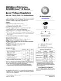
Transcription of MMBZ5221BLT1 - Zener Voltage Regulators
1 Semiconductor Components Industries, LLC, 2001 October, 2016 Rev. 131 Publication Order Number:MMBZ5221 BLT1/DMMBZ52xxBLT1G Series,SZMMBZ52xxBLT1G SeriesZener Voltage Regulators225 mW SOT 23 Surface MountThis series of Zener diodes is offered in the convenient, surfacemount plastic SOT 23 package. These devices are designed to providevoltage regulation with minimum space requirement. They are wellsuited for applications such as cellular phones, hand held portables,and high density PC 225 mW Rating on FR 4 or FR 5 Board Zener Voltage Range V to 91 V Package Designed for Optimal Automated Board Assembly Small Package Size for High Density Applications ESD Rating of Class 3 (> 16 KV) per Human Body Model SZ Prefix for Automotive and Other Applications Requiring UniqueSite and Control Change Requirements.
2 AEC Q101 Qualified andPPAP Capable These Devices are Pb Free, Halogen Free/BFR Free and are RoHSCompliantMechanical CharacteristicsCASE: Void-free, transfer-molded, thermosetting plastic caseFINISH: Corrosion resistant finish, easily solderableMAXIMUM CASE TEMPERATURE FOR SOLDERING PURPOSES:260 C for 10 SecondsPOLARITY: Cathode indicated by polarity bandFLAMMABILITY RATING: UL 94 V 0 MAXIMUM RATINGSR atingSymbolMaxUnitsTotal Power Dissipation on FR 5 Board,(Note 1) @ TA = 25 CDerated above 25 CThermal Resistance,Junction to AmbientRqJA556 C/WTotal Power Dissipation on AluminaSubstrate, (Note 2) @ TA = 25 CDerated above 25 CThermal Resistance,Junction to AmbientRqJA417 C/WJunction and StorageTemperature RangeTJ, Tstg 65 to +150 CStresses exceeding those listed in the Maximum Ratings table may damage thedevice. If any of these limits are exceeded, device functionality should not beassumed, damage may occur and reliability may be FR 5 = X X Alumina = X X in, ORDERING INFORMATIONSOT 23 CASE 318 STYLE 83 Cathode1 AnodeMARKING DIAGRAMSee specific marking information in the device markingcolumn of the Electrical Characteristics table on page 3 ofthis data MARKING INFORMATIONMMMBZ52xxBLT1 GSOT 23(Pb Free)3,000 / Tape & Reel For information on tape and reel specifications,including part orientation and tape sizes, pleaserefer to our Tape and Reel Packaging SpecificationsBrochure, BRD8011 23(Pb Free)10,000 / Tape & Reelxxx GGxxx= Specific Device CodeM= Date CodeG= Pb Free PackageSZMMBZ52xxBLT1 GSOT 23(Pb Free)3,000 / Tape & ReelSZMMBZ52xxBLT3 GSOT 23(Pb Free)10,000 / Tape & Reel(Note.)
3 Microdot may be in either location) Series, SZMMBZ52xxBLT1G CHARACTERISTICS(Pinout: 1-Anode, 2-No Connection, 3-Cathode) (TA = 25 Cunless otherwise noted, VF = V Max. @ IF = 10 mA)SymbolParameterVZReverse Zener Voltage @ IZTIZTR everse CurrentZZTM aximum Zener Impedance @ IZTIZKR everse CurrentZZKM aximum Zener Impedance @ IZKIRR everse Leakage Current @ VRVRR everse VoltageIFForward CurrentVFForward Voltage @ IFZener Voltage RegulatorIFVIIRIZTVRVZVFMMBZ52xxBLT1G Series, SZMMBZ52xxBLT1G CHARACTERISTICS (Pinout: 1-Anode, 2-NC, 3-Cathode) (VF = V Max @ IF = 10 mA for all types.)Device*DeviceMarkingZener Voltage (Note 3) Zener ImpedanceLeakage CurrentVZ (Volts)@ IZTZZT @ IZTZZK @ IZKIR @ parametric performance is indicated in the Electrical Characteristics for the listed test conditions, unless otherwise noted. Productperformance may not be indicated by the Electrical Characteristics if operated under different Zener Voltage is measured with a pulse test current IZ at an ambient temperature of 25 CNOTE:MMBZ5233 BLT1G, MMBZ5246 BLT1G, MMBZ5251 BLT1G, and MMBZ5252 BLT1G Not Available in 10,000/Tape & Reel.
4 *Include SZ-prefix devices where Series, SZMMBZ52xxBLT1G CHARACTERISTICSVZ, TEMPERATURE COEFFICIENT (mV/ C) VZ, NOMINAL Zener Voltage (V)- 3- 2-101234567812111098765432 Figure 1. Temperature Coefficients(Temperature Range 55 C to +150 C)TYPICAL TC VALUESFOR MMBZ52xxBLT1G SERIESVZ @ IZTVZ, TEMPERATURE COEFFICIENT (mV/ C) 10010110100VZ, NOMINAL Zener Voltage (V)Figure 2. Temperature Coefficients(Temperature Range 55 C to +150 C)TYPICAL TC VALUESFOR MMBZ52xxBLT1G SERIESVZ @ IZT100VZ, NOMINAL Zener VOLTAGEF igure 3. Effect of Zener Voltage onZener Impedance101 ZZT, DYNAMIC IMPEDANCE ( ) 1000100101TJ = 25 CIZ(AC) = IZ(DC)f = 1 kHzIZ = 1 mA5 mA20 mAVF, FORWARD Voltage (V)Figure 4. Typical Forward , FORWARD CURRENT (mA)100010010175 V (MMBZ5267 BLT1G)91 V (MMBZ5270 BLT1G)150 C75 C25 C0 CMMBZ52xxBLT1G Series, SZMMBZ52xxBLT1G CHARACTERISTICSC, CAPACITANCE (pF)100VZ, NOMINAL Zener Voltage (V)Figure 5.
5 Typical Capacitance1000100101101 BIAS AT50% OF VZ NOMTA = 25 C0 V BIAS1 V BIAS12VZ, Zener Voltage (V) = 25 CIZ, Zener CURRENT (mA)VZ, Zener Voltage (V) = 25 CIR, LEAKAGE CURRENT ( A) 90VZ, NOMINAL Zener Voltage (V)Figure 6. Typical Leakage +150 C+25 C 55 CIZ, Zener CURRENT (mA)Figure 7. Zener Voltage versus Zener Current(VZ Up to 12 V)Figure 8. Zener Voltage versus Zener Current(12 V to 91 V)MMBZ52xxBLT1G Series, SZMMBZ52xxBLT1G DIMENSIONSSOT 23 (TO 236)CASE 318 08 ISSUE ARDA1312 NOTES:1. DIMENSIONING AND TOLERANCING PER ASME , CONTROLLING DIMENSION: MAXIMUM LEAD THICKNESS INCLUDES LEAD FINISH. MINIMUM LEAD THICKNESS IS THE MINIMUM THICKNESS OFTHE BASE DIMENSIONS D AND E DO NOT INCLUDE MOLD FLASH,PROTRUSIONS, OR GATE FOOTPRINT*VIEW VIEW 100 10T T3 XTOP VIEWSIDE VIEWEND : *For additional information on our Pb Free strategy and solderingdetails, please download the ON Semiconductor Soldering andMounting Techniques Reference Manual, 8:PIN 1.
6 ANODE2. NO CONNECTION3. CATHODEON Semiconductor and are trademarks of Semiconductor Components Industries, LLC dba ON Semiconductor or its subsidiaries in the United States and/or other Semiconductor owns the rights to a number of patents, trademarks, copyrights, trade secrets, and other intellectual property. A listing of ON Semiconductor s product/patent coveragemay be accessed at ON Semiconductor reserves the right to make changes without further notice to any products Semiconductor makes no warranty, representation or guarantee regarding the suitability of its products for any particular purpose, nor does ON Semiconductor assume any liabilityarising out of the application or use of any product or circuit, and specifically disclaims any and all liability, including without limitation special, consequential or incidental damages.
7 Buyeris responsible for its products and applications using ON Semiconductor products, including compliance with all laws, regulations and safety requirements or standards, regardless ofany support or applications information provided by ON Semiconductor. Typical parameters which may be provided in ON Semiconductor data sheets and/or specifications can anddo vary in different applications and actual performance may vary over time. All operating parameters, including Typicals must be validated for each customer application by customer stechnical experts. ON Semiconductor does not convey any license under its patent rights nor the rights of others. ON Semiconductor products are not designed, intended, or authorizedfor use as a critical component in life support systems or any FDA Class 3 medical devices or medical devices with a same or similar classification in a foreign jurisdiction or any devicesintended for implantation in the human body.
8 Should Buyer purchase or use ON Semiconductor products for any such unintended or unauthorized application, Buyer shall indemnify andhold ON Semiconductor and its officers, employees, subsidiaries, affiliates, and distributors harmless against all claims, costs, damages, and expenses, and reasonable attorney feesarising out of, directly or indirectly, any claim of personal injury or death associated with such unintended or unauthorized use, even if such claim alleges that ON Semiconductor wasnegligent regarding the design or manufacture of the part. ON Semiconductor is an Equal Opportunity/Affirmative Action Employer. This literature is subject to all applicable copyrightlaws and is not for resale in any ORDERING INFORMATIONN. American Technical Support: 800 282 9855 Toll FreeUSA/CanadaEurope, Middle East and Africa Technical Support:Phone: 421 33 790 2910 Japan Customer Focus CenterPhone: 81 3 5817 1050 MMBZ5221 BLT1/DLITERATURE FULFILLMENT:Literature Distribution Center for ON Semiconductor19521 E.
9 32nd Pkwy, Aurora, Colorado 80011 USAP hone: 303 675 2175 or 800 344 3860 Toll Free USA/CanadaFax: 303 675 2176 or 800 344 3867 Toll Free USA/CanadaEmail: Semiconductor Website: Literature: additional information, please contact your localSales Representative