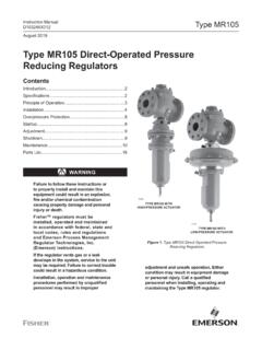
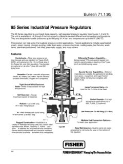
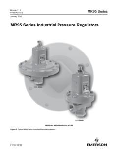
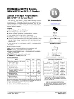
Transcription of MMSZ4678T1 - Zener Voltage Regulators
1 MMSZ4xxxT1G Series, SZMMSZ4xxxT1G Series Zener Voltage Regulators 500 mW, Low IZT SOD 123 Surface Mount Three complete series of Zener diodes are offered in the convenient, surface mount plastic SOD 123 package. These devices provide a convenient alternative to the leadless 34 package style. Features 500 mW Rating on FR 4 or FR 5 Board Wide Zener Reverse Voltage Range V to 43 V. Low Reverse Current (IZT) 50 mA SOD 123. CASE 425. Package Designed for Optimal Automated Board Assembly STYLE 1. Small Package Size for High Density Applications ESD Rating of Class 3 (> 16 kV) per Human Body Model SZ Prefix for Automotive and Other Applications Requiring Unique 1 2. Site and Control Change Requirements; AEC Q101 Qualified and Cathode Anode PPAP Capable These Devices are Pb Free and are RoHS Compliant* MARKING DIAGRAM. Mechanical Characteristics: CASE: Void-free, transfer-molded, thermosetting plastic case 1 xx M G.
2 FINISH: Corrosion resistant finish, easily solderable G. MAXIMUM CASE TEMPERATURE FOR SOLDERING PURPOSES: 260 C for 10 Seconds POLARITY: Cathode indicated by polarity band xx = Device Code (Refer to page 3). FLAMMABILITY RATING: UL 94 V 0 M = Date Code G = Pb Free Package (Note: Microdot may be in either location). MAXIMUM RATINGS. Rating Symbol Max Units ORDERING INFORMATION. Total Power Dissipation on FR 5 Board, PD Device Package Shipping . (Note 1) @ TL = 75 C 500 mW. Derated above 75 C mW/ C MMSZ4xxxT1G SOD 123 3,000 /. (Pb Free) Tape & Reel Thermal Resistance, (Note 2) RqJA C/W. Junction to Ambient 340 SZMMSZ4xxxT1G SOD 123 3,000 /. (Pb Free) Tape & Reel Thermal Resistance, (Note 2) RqJL C/W. Junction to Lead 150 MMSZ4xxxT3G SOD 123 10,000 /. (Pb Free) Tape & Reel Junction and Storage Temperature Range TJ, Tstg 55 to C. +150 SZMMSZ4xxxT3G SOD 123 10,000 /. (Pb Free) Tape & Reel Stresses exceeding those listed in the Maximum Ratings table may damage the device.
3 If any of these limits are exceeded, device functionality should not be For information on tape and reel specifications, assumed, damage may occur and reliability may be affected. including part orientation and tape sizes, please 1. FR 5 = X inches, using the minimum recommended footprint. refer to our Tape and Reel Packaging Specifications 2. Thermal Resistance measurement obtained via infrared Scan Method. Brochure, BRD8011/D. DEVICE MARKING INFORMATION. See specific marking information in the device marking column of the Electrical Characteristics table on page 3 of *For additional information on our Pb Free strategy and soldering details, please this data sheet. download the ON Semiconductor Soldering and Mounting Techniques Reference Manual, SOLDERRM/D. Semiconductor Components Industries, LLC, 2013 1 Publication Order Number: April, 2018 Rev. 12 MMSZ4678T1 /D. MMSZ4xxxT1G Series, SZMMSZ4xxxT1G Series ELECTRICAL CHARACTERISTICS (TA = 25 C unless I.)
4 Otherwise noted, VF = V Max. @ IF = 10 mA). IF. Symbol Parameter VZ Reverse Zener Voltage @ IZT. IZT Reverse Current IR Reverse Leakage Current @ VR VZ VR. V. IR VF. VR Reverse Voltage IZT. IF Forward Current VF Forward Voltage @ IF. Product parametric performance is indicated in the Electrical Characteristics for the listed test conditions, unless otherwise noted. Product performance may not be indicated by the Electrical Characteristics if operated under different conditions. Zener Voltage Regulator 2. MMSZ4xxxT1G Series, SZMMSZ4xxxT1G Series ELECTRICAL CHARACTERISTICS (TA = 25 C unless otherwise noted, VF = V Max. @ IF = 10 mA). Zener Voltage (Note 3) Leakage Current VZ (Volts) @ IZT IR @ VR. Device Device* Marking Min Nom Max mA mA Volts MMSZ4678T1G CC 50 1. MMSZ4679T1G CD 50 5 1. MMSZ4680T1G CE 50 4 1. MMSZ4681T1G CF 50 2 1. MMSZ4682T1G CH 50 1 1. MMSZ4683T1G CJ 50 1. MMSZ4684T1G CK 50 MMSZ4685T1G CM 50 2.
5 MMSZ4686T1G CN 50 5 2. MMSZ4687T1G CP 50 4 2. SZMMSZ4687T1G CG6 50 4 2. MMSZ4688T1G CT 50 10 3. MMSZ4689T1G CU 50 10 3. MMSZ4690T1G/T3G CV 50 10 4. MMSZ4691T1G CA 50 10 5. MMSZ4692T1G CX 50 10 MMSZ4693T1G CY 50 10 MMSZ4694T1G CZ 50 1 MMSZ4695T1G DC 50 1 MMSZ4696T1G DD 50 1 MMSZ4697T1G DE 10 50 1 MMSZ4698T1G DF 11 50 MMSZ4699T1G DH 12 50 MMSZ4700T1G DJ 13 50 MMSZ4701T1G DK 14 50 MMSZ4702T1G DM 15 50 MMSZ4703T1G DN 16 50 MMSZ4704T1G DP 17 50 MMSZ4705T1G DT 18 50 MMSZ4706T1G DU 19 50 MMSZ4707T1G DV 20 50 MMSZ4708T1G DA 22 50 MMSZ4709T1G DX 24 50 MMSZ4710T1G DY 25 50 MMSZ4711T1G EA 27 50 MMSZ4712T1G EC 28 50 MMSZ4713T1G ED 30 50 MMSZ4714T1G EE 33 50 MMSZ4715T1G EF 36 50 MMSZ4716T1G EH 39 50 MMSZ4717T1G EJ 43 50 3. Nominal Zener Voltage is measured with the device junction in thermal equilibrium at TL = 30 C 1 C. *Include SZ-prefix devices where applicable. MMSZ4703 and MMSZ4711 Not Available in 10,000/Tape & Reel 3.
6 MMSZ4xxxT1G Series, SZMMSZ4xxxT1G Series TYPICAL CHARACTERISTICS. 8 100. VZ, TEMPERATURE COEFFICIENT (mV/ C). VZ, TEMPERATURE COEFFICIENT (mV/ C). 7 TYPICAL TC VALUES. 6 TYPICAL TC VALUES. 5. 4 VZ @ IZT VZ @ IZT. 3. 10. 2. 1. 0. -1. - 2. - 3 1. 2 3 4 5 6 7 8 9 10 11 12 10 100. VZ, NOMINAL Zener Voltage (V) VZ, NOMINAL Zener Voltage (V). Figure 1. Temperature Coefficients Figure 2. Temperature Coefficients (Temperature Range 55 C to +150 C) (Temperature Range 55 C to +150 C). 1000. PD, POWER DISSIPATION (WATTS). Ppk , PEAK SURGE POWER (WATTS). RECTANGULAR. WAVEFORM, TA = 25 C. PD versus TL 100. PD versus TA. 10. 0 1. 0 25 50 75 100 125 150 1 10 100 1000. T, TEMPERATURE (5C) PW, PULSE WIDTH (ms). Figure 3. Steady State Power Derating Figure 4. Maximum Nonrepetitive Surge Power 1000. TJ = 25 C. IZ(AC) = IZ(DC). Z ZT, DYNAMIC IMPEDANCE ( ). IZ = 1 mA f = 1 kHz 100. 5 mA. 20 mA. 10. 1. 1 10 100.
7 VZ, NOMINAL Zener Voltage . Figure 5. Effect of Zener Voltage on Zener Impedance 4. MMSZ4xxxT1G Series, SZMMSZ4xxxT1G Series TYPICAL CHARACTERISTICS. 1000 1000. I R , LEAKAGE CURRENT ( A). TA = 25 C. 0 V BIAS 100. 1 V BIAS. 10. C, CAPACITANCE (pF). 100. 1. BIAS AT +150 C. 50% OF VZ NOM. 10. + 25 C. - 55 C. 1 1 10 100 0 10 20 30 40 50 60 70 80 90. VZ, NOMINAL Zener Voltage (V) VZ, NOMINAL Zener Voltage (V). Figure 6. Typical Capacitance Figure 7. Typical Leakage Current 100 100. TA = 25 C TA = 25 C. I Z , Zener CURRENT (mA). I Z , Zener CURRENT (mA). 10 10. 1 1. 0 2 4 6 8 10 12 10 30 50 70 90. VZ, Zener Voltage (V) VZ, Zener Voltage (V). Figure 8. Zener Voltage versus Zener Current Figure 9. Zener Voltage versus Zener Current (VZ Up to 12 V) (12 V to 91 V). 5. MECHANICAL CASE OUTLINE. PACKAGE DIMENSIONS. SOD 123. CASE 425 04. ISSUE G. DATE 07 OCT 2009. SCALE 5:1. D. A NOTES: 1. DIMENSIONING AND TOLERANCING PER ANSI.
8 A1 , 1982. 2. CONTROLLING DIMENSION: INCH.. 1. MILLIMETERS INCHES.. DIM MIN NOM MAX MIN NOM MAX. A A1 b HE E c --- --- --- --- D E HE L --- --- --- --- q 0 --- 10 0 --- 10 . 2. q GENERIC. b L MARKING DIAGRAM*. C. XXXMG. 1. SOLDERING FOOTPRINT* G. XXX = Specific Device Code . M = Date Code . G = Pb Free Package (Note: Microdot may be in either location). *This information is generic. Please refer to device data sheet for actual part marking. Pb Free indicator, G or microdot G , may or may not be present. STYLE 1: PIN 1. CATHODE. 2. ANODE. SCALE 10:1 inches mm . *For additional information on our Pb Free strategy and soldering details, please download the ON Semiconductor Soldering and Mounting Techniques Reference Manual, SOLDERRM/D. DOCUMENT NUMBER: 98 ASB42927B Electronic versions are uncontrolled except when accessed directly from the Document Repository. Printed STATUS: ON SEMICONDUCTOR STANDARD versions are uncontrolled except when stamped CONTROLLED COPY in red.
9 NEW STANDARD: Semiconductor Components Industries, LLC, 2002 Case Outline Number: October, DESCRIPTION: 2002 Rev. 0 SOD 123 1 PAGE 1 OFXXX2. DOCUMENT NUMBER: 98 ASB42927B. PAGE 2 OF 3. ISSUE REVISION DATE. D CHANGED OWNERSHIP TO ON SEMI. 16 MAR 2000. E ADDED NOMINAL VALUES AND SOLDERING FOOTPRINT. REQ. BY H XIAO. 03 AUG 2005. F ADDED FOOT ANGLE TO DRAWING. REQ. BY D. TRUHITTE. 14 AUG 2009. G ADJUSTED DIMENSION L LABEL TO MORE ACCURATELY REFLECT FOOT 07 OCT 2009. LENGTH. REQ. D. TRUHITTE. ON Semiconductor and are registered trademarks of Semiconductor Components Industries, LLC (SCILLC). SCILLC reserves the right to make changes without further notice to any products herein. SCILLC makes no warranty, representation or guarantee regarding the suitability of its products for any particular purpose, nor does SCILLC assume any liability arising out of the application or use of any product or circuit, and specifically disclaims any and all liability, including without limitation special, consequential or incidental damages.
10 Typical parameters which may be provided in SCILLC data sheets and/or specifications can and do vary in different applications and actual performance may vary over time. All operating parameters, including Typicals must be validated for each customer application by customer's technical experts. SCILLC does not convey any license under its patent rights nor the rights of others. SCILLC products are not designed, intended, or authorized for use as components in systems intended for surgical implant into the body, or other applications intended to support or sustain life, or for any other application in which the failure of the SCILLC product could create a situation where personal injury or death may occur. Should Buyer purchase or use SCILLC products for any such unintended or unauthorized application, Buyer shall indemnify and hold SCILLC and its officers, employees, subsidiaries, affiliates, and distributors harmless against all claims, costs, damages, and expenses, and reasonable attorney fees arising out of, directly or indirectly, any claim of personal injury or death associated with such unintended or unauthorized use, even if such claim alleges that SCILLC was negligent regarding the design or manufacture of the part.