Transcription of MOSFETs in the Sub-threshold Region (i.e. a bit below VT)
1 MOSFETs in the Sub-threshold Region ( a bit below VT) Clifton Fonstad, 10/28/09 In the depletion approximation for n-channel MOS structures we have neglected the electrons beneath the gate electrode when the gate voltage is less than the threshold voltage, VT. We said that it is only when the gate voltage is above threshold that they are significant, and that they are then the dominant negative charge under the gate. Furthermore, we say that above threshold all of the gate voltage in excess of VT induces electrons in the channel; thus our model is that the sheet charge density under the gate, qN*, is ! qN"=0 for vGC#VT$oxtoxvGC%VT() for VT#vGC& ' ( ) ( (1)As MOS integrated circuit technology has evolved to exploit smaller and smaller device structures, it has become increasingly important in recent years to look more closely at the minority carriers present under the gate when the gate voltage is less than threshold, in what is called the Sub-threshold Region .)
2 These carriers cannot be totally neglected, and play an important role in device and circuit performance. At first they were viewed primarily as a problem, causing undesirable leakage currents and limiting circuit performance. Now it is recognized that they also enable a very useful mode of MOSFET operation, and that the Sub-threshold Region of operation is as important as the traditional cut-off, linear, and saturations regions of operation. To begin our study of the Sub-threshold Region , we will first quickly review the electrostatics of the MOS capacitor, and the electrostatic potential profile predicted by the depletion approximation model. Then we will use this result to derive a more accurate expression than that in Equation 1 for qN* below threshold, and use the resulting expression to, among other things, assess the assumption that the contribution of the mobile electrons underneath the gate to the net charge density in the depletion Region is negligible compared to the contribution from the ionized acceptors.
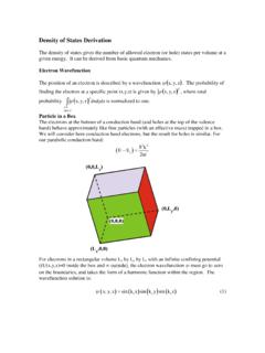
3 Finally we will look at the current-voltage characteristic of a MOSFET operating in the Sub-threshold Region , and merge it with our earlier model so that we then have a model in which the mobile electron charge is taken into account and the drain current is no longer identically zero when vGS is less than VT. Supplementary Notes: MOSFETs in the Sub-threshold Region ( a bit below VT) The Electrostatics of the MOS Capacitor with vBC = 0 Consider the MOS capacitor with vBC = 0 illustrated in Figure 1, the same structure we used when we first looked at the MOS capacitor using the depletion approximation. In the depletion p-Sin+BCGSiO2+ vGC(= vGB)FIGURE 1 A MOS capacitor connected as a two-terminal capacitor with vGC = vGB = 0. approximation, we assume that Equation 1 holds and that the net charge density profile, (x), under the gate for VFB < vGC < VT can be approximated as: ! "(x)=qNA for 0#x#xD0for xD#x$ % & (2)With this assumption, we found that the electrostatic potential profile is: !
4 "(x)="p+qNAx#xD()22$Si for 0%x%xD"p for xD%x& ' ( ) ( (3)This expression is plotted in Figure 2, which also continues the plot through the oxide to the gate, from which we can also get the expression relating the depletion Region width, xD, to vGB and VFB: ! vGB"VFB=qNAxDtox#ox+ qNAxD22#Si (4)2 Supplementary Notes: MOSFETs in the Sub-threshold Region ( a bit below VT) FIGURE 2 A sketch of (x) from the metal on the left, t hrough the oxide, a nd into the p-type semiconductor in an n-channel MOS capacitor for an applied gate bias, vGB, in the weak-inversion, Sub-threshold Region . Equation 4 is useful because it can be solved explicitly for xD, and the result can be used to obtain an expression for (x) as a function of vGB. However, it will turn out that what is most important to us is (0), the value of the potential at the interface, and (0) is much easier to relate to vGB than is (x) at an arbitrary x.)
5 To do so we first find xD in terms of (0): ! xD=2"Si#(0)$#p[]qNA (5)Using this in Equation 4 gives us an equation relating (0) and vGB that will be useful to us shortly: ! vGB"VFB=tox#ox2#SiqNA$(0)-$p[]+ $(0)-$p[] (6) Sub-threshold Electron Sheet Charge density , vGC = 0 Returning to our original goal, which was to find the electron population density , n(x), under the gate, and then the electron sheet charge density , qN*, we note that the Boltzman relationship between the electrostatic potential and carrier population holds under the gate of the MOS capacitor in Figure 1 because the current in the x-direction is zero. Thus we have: 3 Supplementary Notes: MOSFETs in the Sub-threshold Region ( a bit below VT) ! n(x,vGB)=nie"x,vGB()"t (7a) =ni2 NAe"x,vGB()#"p[]"t (7b)p(x,vGB)=nie#"x,vGB()"t (8a) =NAe#"x,vGB()#"p[]"t (8b)In these equations we use t for the thermal voltage, kT/q, and we have indicated the dependency on vGB to emphasize that these populations depend on the gate voltage as well as on position, x.
6 To obtain the Equations 7b and 8b, we have used po = NA = ni exp(- p/ t) to get expressions explicitly including the quantity [ (x,vGB) - p], which also appears in Eqs. 5 and 6. Note: In many texts, [ (0,vGB) - p] is identified as VB(vGB), the voltage drop between the silicon bulk and the oxide-silicon interface, VB(vGB) [ (0,vGB) - p]. We can calculate the electron sheet charge density , qN*, by multiplying n(x) by q and integrating with respect to x from the interface, x = 0, into the silicon until x = xi, where xi is defined as the depth at which (x) = 0, and thus where we have n(xi) = p(xi) = ni: ! qN"vGB()=#qn(x,vGB)dx0xivGB()$ (9a) =#qnie%x,vGB()%tdx0xivGB()$ (9b) =#qni2 NAe%x,vGB()#%p[]%tdx0xivGB()$ (9c)The end-point x = xi is used for the integration because for x > xi, p(x) > n(x) and the material is still p-type, while for x < xi, n(x) > p(x) and the material net n-type and is said to be weakly inverted.
7 This is actually a minor point, however, and not worth fretting about, because n(x) falls off very rapidly with increasing x, and the main contributions to the integral come from the Region near the interface ( small x) where (x) is near (0). The integral itself will be significant only when (0) approaches p, which further reduces the importance of the tail, and how far from the interface one integrates. The next step in calculating qN* would seem to be to replace (x) in Eq. 9c with an explicit function of x so we can do the integral. We can do this using Eq. 3, and we find 4 Supplementary Notes: MOSFETs in the Sub-threshold Region ( a bit below VT) ! qN"vGB()=#qni2 NAeqNAx-xDvGB()[]22$Si%tdx0xivGB()& (10)This integral is clearly difficult to evaluate, however, without resorting to numerical techniques, a less than optimum situation. An alternative approach is to make use of our earlier observation that the main contribution to the integral occurs near x = 0, and to further note that near x = 0 the potential variation with x is nearly linear.
8 A bit of algebra gives us ! "x,vGB()="0,vGB()#qNA2$Si2xDvGB()#x[]%x (11a) & "0,vGB()#qNAxDvGB()$Si%x (11b) & "0,vGB()#2qNA"0,vGB()#"p[]$Si%x (11c)Using this approximation in the Eq. 9c yields an analytical expression which does not obscure the dependences on material properties ! qN"#()$%qni2#tNA&Si2qNA#0,vGB()%#p[]e#0, vGB()%#p[]#t for #0,vGB()'%#p vGB'VT (12)Note that in the range validity, (0,vGB) - p, c orresponds to gate voltages such that vGB VT. To see if the Sub-threshold charge is large or small relative to the channel charge which develops above threshold [ , qN*(vGB) = Cox *(vGB-VT)], one can evaluate Eq. 12 for values of (0,vGB) near threshold, say for example (- p -10 t) to - p. The corresponding values of vGB can be found using Eq. 6, and then one can plot qN* verses vGB in the vicinity of vGB = VT; the result is shown in Figure 3 for a MOS capacitor with NA = 1018 cm -3 and tox = 3 nm.
9 Note that the weak-inversion charge does not increase further above threshold, but instead is pinned at the value it reaches when vGB = VT. (This value is x 10-9 Coul/cm2 for the specific values of NA and tox used in Figure 3). The first thing to note in Figure 3 is that the range of gate voltages where the Sub-threshold charge is significant in this example is from about 50 mV below threshold to threshold. Note also that neglecting the Sub-threshold charge only leads to a 6 mV error in the threshold, VT, that 5 Supplementary Notes: MOSFETs in the Sub-threshold Region ( a bit below VT) FIGURE 3 The electron sheet charge density under the gate with a gate voltage in the vicinity of threshold. The blue curve corresponds to the Sub-threshold weak-inversion charge [Eq. 12], and the red curve is the strong inversion charge from traditional depletion approximation modeling [Eq. 1]. The sum is plotted in the yellow curve. would be extrapolated from a C-V measurement; thus, taking the Sub-threshold electron charge into account makes only a very minor correction to the predicted value of Volts.
10 Another way to get a feel for the relative significance, or insignificance, of the Sub-threshold electron charge is to compare it to the sheet charge in the depletion Region at threshold, qNAXD = (2 Si|2 p|qNA)1/2. A quick calculation shows that this charge is x 10-7 coul/cm2, which is about 70 times larger than qN*(VT). Returning to our expression for the charge under the gate below threshold, Eq. 12, we next take the derivation one step further to express qN* explicitly in terms of vGB. One way to do this is to return to Eq. 6 and solve it for (0,vGB), which yields 6 Supplementary Notes: MOSFETs in the Sub-threshold Region ( a bit below VT) ! "(0,vGB)="p+2#SiqNA#oxtox()21+vGB$VFB2#S iqNA#oxtox()2$1% & ' ' ( ) * * 2 (13)Putting this into Eq. 12 clearly won t lead to an equation that gives one much insight, so it seems worthwhile to look into making simplifying approximations before proceeding, particularly since we know from Figure 3 that the most important Region is the small range of voltages below vGB = VT, (0) = - p.