Transcription of Multiple-Bit Wire Naming Conventions
1 Virtuoso Schematic Composer User GuideUnderstanding Connectivity and Naming ConventionsApril 2001110 Product Version wire Naming ConventionsYou can connect Multiple-Bit wires in your design using any one of the following namingconventions: Using Vector Expressions in Multiple-Bit wire Names on page 110 Using Vector Expressions in multiple Signals on page 110 Evaluating Vector Expressions in Multiple-Bit wire Names on page 111 Using Prefix Repeat Operators in Multiple-Bit wire Names on page 111 Using Suffix Repeat Operators in Multiple-Bit wire Names on page 112 Using Vector Expressions in Multiple-Bit wire NamesA Multiple-Bit wire name can be a bundle, a bus, or a combination of the two.
2 You can improvereadability in your designs by shortening Multiple-Bit wire indicate that multiple bits of one wire carry similar information, give each bit the same basename. Then add a suffix to each bit name to distinguish the example, to show four bits of a wire with a common base name (DATA), but with individualsuffixes (<0>,<1>,<2>, and<3>), assign the following names:DATA<0>,DATA<1>,DATA<2>, and DATA<3>.Using Vector Expressions in multiple SignalsTo name a wire that contains multiple signals with the same base name, specify the basename followed by a vector expression. The vector expression can be A list of the individual bit numbers separated by commas and enclosed with example,DATA<2,1,0> representsDATA<2>,DATA<1>, andDATA<0>.
3 A range of numbers containing a lower and upper bound and, optionally, an incrementvalue. The numbers are separated with colons and enclosed with angle example,DATA<1:7:2> representsbaseName <lowerBound :upperBound : [incrValue]>Use a positive integer forincrValue. If you do not specify an increment value, theeditor Schematic Composer User GuideUnderstanding Connectivity and Naming ConventionsApril 2001111 Product Version ordering of the bits in a bus is important when you are connecting the bus to a pin thathas a width greater than Vector Expressions in Multiple-Bit wire NamesThe system evaluates vector expressions in Multiple-Bit wire names as follows: The vector expressionDATA<0:3:2> names a 2-bit bus containingDATA<0>andDATA<2>.
4 The vector expressionDATA<1:3:2> names a 2-bit bus containingDATA<1> andDATA<3>. The vector expressionsDATA<0:3> andDATA<0:3:1> are equivalent names thatgenerate a 4-bit bus containingDATA<0>,DATA<1>,DATA<2>, andDATA<3>.If the lower bound is larger than the upper bound , the editor generates the bit numbers indescending order, as follows: The vector expressionDATA<2:0> generates a 3-bit bus that containsDATA<2>,DATA<1>, andDATA<0>.Using Prefix Repeat Operators in Multiple-Bit wire NamesA Multiple-Bit wire name can be a bundle, a bus, or a combination of the two. You can improvereadability in your designs by shortening Multiple-Bit wire can repeat a single signal name, a group of signal names, or a vector term any numberof times in the wire name by placing a prefix repeat operator<*n>in front of the name, wheren is a positive integer that defines the number of times to repeat each bit in the vector term.
5 Use the prefix repeat operator<*n> to repeat a single-signal name. The followingequivalent wire names both name the same four-bit wire :<*2>A,B,CA,A,B,C Use the prefix repeat operator<*n>and parentheses to repeat a group of signal following two wire names are equivalent:<*2>(A,B),CA,B,A,B,C Use combinations of the prefix repeat operator<*n> and parentheses to nestparenthetical expressions to any required depth. The editor expands nested expressionsfrom the innermost expression outward . For example, a name with the expression<*2>(A,<*2>(X,Y)),B expands toA,X,Y,X,Y,A,X,Y,X,Y, Schematic Composer User GuideUnderstanding Connectivity and Naming ConventionsApril 2001112 Product Version Suffix Repeat Operators in Multiple-Bit wire NamesA Multiple-Bit wire name can be a bundle, a bus, or a combination of the two.
6 You can improvereadability in your designs by shortening Multiple-Bit wire names using vector suffix repeat operator is a number,<*n>, after a vector term, wherenis a positive integerthat defines the number of times to repeat each bit in the vector term. Use the suffix repeat operator<*n> to repeat each bit in a group of bit names beforeexpanding the vector term. For example, the following three names all describe the samesix-bit wire :A<0:2*2>A<0*2,1*2,2*2>A<0,0,1,1,2,2> Use the suffix repeat operator<*n> and parentheses to repeat the sequence of bitnames. In this case, the vector term is expanded before the bits are repeated. Thefollowing names all describe the same six-bit wire :A<(0:2)*2>A<0:2,0:2>A<0,1,2,0,1,2>Pin Connections and Pin Naming ConventionsA pin name consists of a string of printable characters.
7 You must observe therules forreserved can name pins in a design To declare which nets in the schematic are connected to a higher level of the designhierarchy To declare which nets span across sheets in a multisheet schematicThis section describes the following pin connections and Naming Conventions : Hierarchical Pin Names on page 113 Offsheet Pin Names on page 113 Bus Pin Names on page 113 Pin-to-Pin Connections on page 114 Tapping Pins on page 114 Virtuoso Schematic Composer User GuideUnderstanding Connectivity and Naming ConventionsApril 2001113 Product Version Pin NamesIf you are designing a multisheet schematic, your sheets contain hierarchical pins andoffsheet pins are pins that also appear on the symbol of the design.
8 The hierarchical pinsfrom each sheet become the hierarchical pins of the Pin NamesOffsheet pins connect signals across the sheets of a multisheet schematic only. Use the samename for the offsheet pins on each you want a signal to appear on a multiple sheet that is also exported by a hierarchical pin,place a hierarchial pin for the first usage and offsheet pins on other sheets. Do not place morethan one hierarchical pin with the same name in a multisheet Pin NamesUse abase name with avector expression. For example,IN<16:10:2> expands to thesefour pins:IN<16>,IN<14>,IN<12>, andIN<10>.IO<0:7>OUT2<0:7>A<0:7>Hierarchical pinOffsheet pinIO<0:7>OUT2<0:7>A<0:7>Hierarchical pinOffsheet pinVirtuoso Schematic Composer User GuideUnderstanding Connectivity and Naming ConventionsApril 2001114 Product Version ConnectionsA direct connection between two instance pins without an intermediate wire is called a pin-to-pin connection.
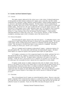
9 There are four ways to make pin-to-pin connections:Tapping PinsYou cannot draw a tap directly from an instance tap a multibit connection to an instance pin, you must attach a wire named with a bus nameto the instance pin. You can then draw taps from the named a schematic pin has a bus name, you can draw a tap directly from the pin using avectorexpression to name a wire that intersects with the 1 Pin 1 Pin 1 Pin 2 Pin 2 Pin 2 Pins overlap overlap is contained withina 2 Pins touch each 1 Virtuoso Schematic Composer User GuideUnderstanding Connectivity and Naming ConventionsApril 2001115 Product Version following figure shows how to tap pins in a the example above, the wire named<7:4> is a tap of the schematic pin namedINPUT<7:0>and connects a four-bit bus calledINPUT<7:4>to the input of the inverter (aniterated instance).
10 The wire named<3:0> is also a tap of theINPUT<7:0> pin and connects a four-bit buscalledINPUT<3:0> to the input of theNAND2 gate (also an iterated instance).If you do not apply a name to a net that is attached to a pin, the editor gives the net the samename as the pin. For example, the wire that connects the output of theNAND2 gate to theOUTPUT<0:3> pin is calledOUTPUT<0:3>.Patchcord Connections and Patchcord NamingConventionsTheschPatchExpr connection expression (value) for patchcords has the following form:src_vector_expression = dst_vector_expressionINPUT<7:4>invnand2 YABOUTPUT<3:0>AY<0:3> <7:0>I1<0:3>I4<0:3> wire namedOUTPUT<0:3>Hierarchical pinHierarchical pinSymbol pinsAB0=0