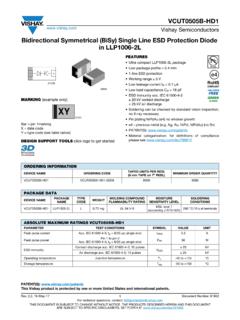
Transcription of N- and P-Channel 20 V (D-S) MOSFET - Vishay
1 Siliconix S14-1130-Rev. B, 02-Jun-141 Document Number: 67693 For technical questions, contact: DOCUMENT IS SUBJECT TO CHANGE WITHOUT NOTICE. THE PRODUCTS DESCRIBED HEREIN AND THIS DOCUMENTARE SUBJECT TO SPECIFIC DISCLAIMERS, SET FORTH AT and P-Channel 20 V (D-S) MOSFETM arking Code: RHOrdering Information:Si1553 CDL-T1-GE3 (Lead (Pb)-free and Halogen-free)FEATURES TrenchFET power MOSFET 100 % Rg tested Material categorization:for definitions of compliance please APPLICATIONS Load switch DC/DC converterNotesa. Based on TC = 25 Surface mounted on 1" x 1" FR4 t = 10 Maximum under steady state conditions is 486 C/W (N- channel ) and 486 C/W ( P-Channel ).
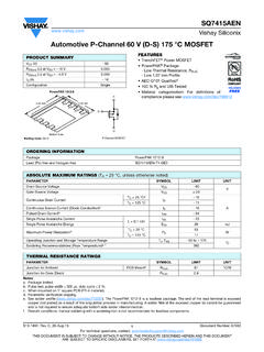
2 PRODUCT SUMMARYVDS (V)RDS(on) ( )ID (A) aQg (TYP.) at VGS = V at VGS = V at VGS = V at VGS = V at VGS = V at VGS = V Dual (6 leads)Top View1S12G13D2D16G25S24N- channel MOSFET D 1 G 1 S 1 S2G2D2P- channel MOSFETABSOLUTE MAXIMUM RATINGS (TA = 25 C, unless otherwise noted)PARAMETER SYMBOL N-CHANNELP-CHANNELUNIT Drain-Source Voltage VDS20-20 VGate-Source Voltage VGS 12 Continuous Drain Current (TJ = 150 C)
3 TC = 25 = 70 = 25 b, b, cTA = 70 b, b, cSource-Drain Current Diode CurrentTC = 25 = 25 b, b, cPulsed Drain Current (t = 300 s)IDM2-1 Maximum Power DissipationTC = 25 = 70 = 25 b, b, cTA = 70 b, b, cOperating Junction and Storage Temperature Range TJ, Tstg-55 to 150 CTHERMAL RESISTANCE RATINGSPARAMETER SYMBOL N-CHANNELP-CHANNELUNIT Junction-to-Ambient b, dt 10 sRthJA365438365438 C/WMaximum Junction-to-Foot (Drain)Steady Siliconix S14-1130-Rev.
4 B, 02-Jun-142 Document Number: 67693 For technical questions, contact: DOCUMENT IS SUBJECT TO CHANGE WITHOUT NOTICE. THE PRODUCTS DESCRIBED HEREIN AND THIS DOCUMENTARE SUBJECT TO SPECIFIC DISCLAIMERS, SET FORTH AT (TJ = 25 C, unless otherwise noted)PARAMETER SYMBOL TEST CONDITIONS StaticDrain-Source Breakdown VoltageVDSVGS = 0 V, ID = 250 A N-Ch20--VVGS = 0 V, ID = -250 A P-Ch-20--VDS Temperature Coefficient VDS/TJID = 250 A N-Ch-24-mV/ CID = -250 A P-Ch--13-VGS(th)
5 Temperature Coefficient VGS(th)/TJ ID = 250 A = -250 A Threshold VoltageVGS(th) VDS = VGS, ID = 250 A = VGS, ID = -250 A LeakageIGSSVDS = 0 V, VGS = 12 V N-Ch-- 100nAP-Ch-- 100 Zero Gate Voltage Drain CurrentIDSSVDS = 20 V, VGS = 0 V N-Ch--1 AVDS = -20 V, VGS = 0 VP-Ch---1 VDS = 20 V, VGS = 0 V, TJ = 55 C N-Ch--10 VDS = -20 V, VGS = 0 V, TJ = 55 C P-Ch---10On-State Drain Current bID(on) VDS = 5 V, VGS = 5 V N-Ch2--AVDS = -5 V, VGS = -5 V P-Ch-1--Drain-Source On-State Resistance bRDS(on) VGS = V, ID = A VGS = V, ID = A = V, ID = A = V, ID = A = V, ID = A = , ID = A Transconductance bgfs VDS = 15 V, ID = A = -15 V, ID = A aInput CapacitanceCissN-ChannelVDS = 10 V, VGS = 0 V, f = 1 MHzP-ChannelVDS = -10 V, VGS = 0 V, f = 1 MHzN-Ch-38-pFP-Ch-43-Output CapacitanceCossN-Ch-14-P-Ch-16-Reverse Transfer CapacitanceCrss N-Ch-6-P-Ch-10-Total Gate ChargeQgVDS = 10 V, VGS = 10 V, ID = A = -10 V, VGS = -10 V, ID = A = 10 V, VGS = V ID = AP-ChannelVDS = -10 V, VGS = V.
6 ID = ChargeQgs ChargeQgd ResistanceRgf = 1 Siliconix S14-1130-Rev. B, 02-Jun-143 Document Number: 67693 For technical questions, contact: DOCUMENT IS SUBJECT TO CHANGE WITHOUT NOTICE. THE PRODUCTS DESCRIBED HEREIN AND THIS DOCUMENTARE SUBJECT TO SPECIFIC DISCLAIMERS, SET FORTH AT Guaranteed by design, not subject to production Pulse test; pulse width 300 s, duty cycle 2 %.Stresses beyond those listed under Absolute Maximum Ratings may cause permanent damage to the device. These are stress ratings only, and functional operationof the device at these or any other conditions beyond those indicated in the operational sections of the specifications is not implied.
7 Exposure to absolute maximumrating conditions for extended periods may affect device aTurn-On Delay Timetd(on) N-ChannelVDD = 10 V, RL = 20 ID A, VGEN = 10 V, Rg = 1 P-ChannelVDD = -10 V, RL = 25 ID A, VGEN = -10 V, Rg = 1 N-Ch-24nsP-Ch-24 Rise TimetrN-Ch-1421P-Ch-918 Turn-Off Delay Timetd(off) N-Ch-1120P-Ch-1020 Fall TimetfN-Ch-714P-Ch-714 Turn-On Delay Timetd(on) N-ChannelVDD = 10 V, RL = 20 ID A, VGEN = V, Rg = 1 P-ChannelVDD = -10 V, RL = 25 ID A, VGEN = V, Rg = 1 N-Ch-1624P-Ch-1523 Rise TimetrN-Ch-2233P-Ch-1523 Turn-Off Delay Timetd(off) N-Ch-2233P-Ch-1220 Fall TimetfN-Ch-1320P-Ch-816 Drain-Source Body Diode CharacteristicsContinuous Source-Drain Diode CurrentISTC = 25 C Diode Forward Current aISMN-Ch--2P-Ch---1 Body Diode VoltageVSDIS = = Diode Reverse Recovery TimetrrN-ChannelIF = A, dI/dt = 100 A/ s, TJ = 25 CP-ChannelIF = A, dI/dt = -100 A/ s, TJ = 25 C N-Ch-815nsP-Ch-1220 Body Diode Reverse Recovery ChargeQrrN-Ch-12nCP-Ch-510 Reverse Recovery Fall TimetaN-Ch-4-nsP-Ch-9-Reverse Recovery Rise TimetbN-Ch-4-P-Ch-3-SPECIFICATIONS (TJ = 25 C, unless otherwise noted)
8 PARAMETER SYMBOL TEST CONDITIONS Siliconix S14-1130-Rev. B, 02-Jun-144 Document Number: 67693 For technical questions, contact: DOCUMENT IS SUBJECT TO CHANGE WITHOUT NOTICE. THE PRODUCTS DESCRIBED HEREIN AND THIS DOCUMENTARE SUBJECT TO SPECIFIC DISCLAIMERS, SET FORTH AT CHARACTERISTICS (25 C, unless otherwise noted)Output CharacteristicsOn-Resistance vs. Drain Current and Gate VoltageGate ChargeTransfer CharacteristicsCapacitanceOn-Resistance vs.
9 Junction Drain Current (A)VDS-Drain-to-Source Voltage (V)VGS= VVGS= 5 V thru 3 VVGS= VVGS= 2 (on)-On-Resistance ( )ID- Drain Current (A)VGS= VVGS= VVGS= V0 2 4 6 8 10 Voltage (V)Qg-Total Gate Charge (nC)VDS= 16 VVDS= 5 VVDS= 10 VID= Drain Current (A)VGS-Gate-to-Source Voltage (V)TC= - 55 CT = 125 CCTC= 25 C0102030405005101520C - Capacitance (pF)VDS-Drain-to-Source Voltage (V) -50 -250255075100125150 RDS(on)-On-Resistance (Normalized)TJ- Junction Temperature ( C)ID= AVGS= VVGS= Siliconix S14-1130-Rev. B, 02-Jun-145 Document Number: 67693 For technical questions, contact: DOCUMENT IS SUBJECT TO CHANGE WITHOUT NOTICE.
10 THE PRODUCTS DESCRIBED HEREIN AND THIS DOCUMENTARE SUBJECT TO SPECIFIC DISCLAIMERS, SET FORTH AT CHARACTERISTICS (25 C, unless otherwise noted)Source-Drain Diode Forward VoltageThreshold VoltageOn-Resistance vs. Gate-to-Source VoltageSingle Pulse Power, Junction-to-AmbientSafe Operating Area, IS-Source Current (A)VSD-Source-to-Drain Voltage (V)TJ= 150 CTJ= 25 255075100125150 VGS(th)(V)TJ-Temperature ( C)ID= 250 (on)-On-Resistance ( )VGS-Gate-to-Source Voltage (V)TJ= 125 CTJ= 25 CID= (W)Time (s) Drain Current (A)VDS-Drain-to-Source Voltage (V)* VGS> minimum VGSat which RDS(on)is specified100 msLimited by RDS(on)*1 msTC= 25 CSingle PulseBVDSS Limited10 ms100 s1 s10 s, Siliconix S14-1130-Rev.
