Transcription of NCP177 - Linear Voltage Regulator, Fast Transient Response ...
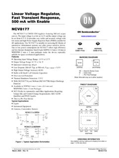
1 Semiconductor Components Industries, LLC, 2017 October, 2020 Rev. 71 Publication Order Number: NCP177 /DLinear Voltage Regulator - fast Transient Response ,Enable500 mANCP177 The NCP177 is CMOS LDO regulator featuring 500 mA outputcurrent. The input Voltage is as low as V and the output Voltage canbe set from Operating Input Voltage Range: V to V Output Voltage Range: V to V Quiescent Current typ. 60 mA Low Dropout: 200 mV Typ. at 500 mA, VOUT NOM = V High Output Voltage Accuracy Stable with Small 1 mF Ceramic Capacitors Over current Protection Thermal Shutdown Protection: 175 C With (NCP177A) and Without (NCP177B) Output DischargeFunction Available in XDFN4 1 mm x 1 mm x mm Package This is a Pb Free DeviceTypical Applications Battery Powered Equipment Portable Communication Equipment Cameras, Image Sensors and CamcordersFigure 1.
2 Typical ApplicationSchematicNCP177 INENOUTGNDCOUT1 FCIN1 FOFFONVINVOUTMARKING DIAGRAMXDFN4 CASE 711 AJSee detailed ordering, marking and shipping information onpage 10 of this data INFORMATION(Top View) = Specific Device CodeM= Date CodeXX M11 PINOUT 2. Internal Block DiagramINENOUTGNDPROG . VOLTAGEREFERENCE ANDSOFT VTHERMALSHUTDOWNNCP177A (with output active discharge)NCP177B (without output active discharge)INENOUTGNDPROG . VOLTAGEREFERENCE ANDSOFT VTHERMALSHUTDOWNPIN FUNCTION DESCRIPTIONPin NameDescription1 OUTR egulated output Voltage pin2 GNDP ower supply ground pin3 ENEnable pin (active H )4 INPower supply input Voltage pin EPADE xposed pad should be tied to ground plane for better power dissipationABSOLUTE MAXIMUM RATINGSR atingSymbolValueUnitInput Voltage (Note 1)IN to VoltageOUT to VIN + Enable InputEN to CurrentIOUTI nternally LimitedmAMaximum Junction TemperatureTJ(MAX)150 CStorage TemperatureTSTG 55 to 150 CESD Capability, Human Body Model (Note 2)ESDHBM2000 VESD Capability, Machine Model (Note 2)ESDMM200 VStresses exceeding those listed in the Maximum Ratings table may damage the device.
3 If any of these limits are exceeded, device functionalityshould not be assumed, damage may occur and reliability may be Refer to ELECTRICAL CHARACTERISTICS and APPLICATION INFORMATION for Safe Operating This device series incorporates ESD protection and is tested by the following methods:ESD Human Body Model tested per JESD22 A114 ESD Machine Model tested per JESD22 A115 Latchup Current Maximum Rating tested per JEDEC standard: JESD78 THERMAL CHARACTERISTICSR atingSymbolValueUnitThermal Characteristics, XDFN4 (Note 3)Thermal Resistance, Junction to AirRqJA223 C/W3. Measured according to JEDEC board specification. Detailed description of the board can be found in JESD51 CHARACTERISTICSVIN = VOUT NOM + V or VIN = V (whichever is higher), VEN = V, IOUT = 1 mA, CIN = COUT = mF, TJ = 25 CThe specifications in bold are guaranteed at 40 C TJ 85 C.
4 (Note 4)ParameterTest ConditionsSymbolMinTypMaxUnitInput VoltageVOUT_NOM VTJ = +25 CVOUT 40 C TJ 85 C < VTJ = +25 C 40 C TJ 85 C RegulationVIN = VOUT NOM + V to VVIN Regulation1 mA IOUT 500 mA, VIN VLoadReg110mVDropout Voltage (Note 5)IOUT = 500 V VOUT < V VOUT < V VOUT < V VOUT < V VOUT < V110175 Quiescent CurrentIOUT = 0 mAIQ6090mAStandby CurrentVEN = 0 Current LimitVOUT = VOUT NOM 100 mV, VIN VIOUT510800mAVOUT = VOUT NOM 100 mV, VIN V300600 Short Circuit CurrentVOUT = 0 V, VIN VISC510800mAEN Pin Threshold VoltageEN Input Voltage H Input Voltage L Input CurrentVEN = VIN = Supply Rejection Ratiof = 1 kHz, Ripple Vp p,VIN = VOUT NOM + V, IOUT = 30 mA(VOUT V, VIN = V)PSRR75dBOutput Noisef = 10 Hz to 100 kHz54mVRMSO utput Discharge Resistance(NCP177A option only)
5 VIN = V, VEN = 0 V, VOUT = VOUT NOMRACTDIS60 WThermal Shutdown TemperatureTemperature rising from 25 CTSD_TEMP175 CThermal Shutdown HysteresisTemperature falling from TSD_TEMPTSD_HYST20 CProduct parametric performance is indicated in the Electrical Characteristics for the listed test conditions, unless otherwise noted. Productperformance may not be indicated by the Electrical Characteristics if operated under different Performance guaranteed over the indicated operating temperature range by design and/or characterization. Production tested at TA = 25 duty cycle pulse techniques are used during the testing to maintain the junction temperature as close to ambient as Measured when the output Voltage falls 3% below the nominal output Voltage (the Voltage measured under the condition VIN = VOUT NOM+ V).
6 CHARACTERISTICSVIN = VOUT NOM + V or VIN = V (whichever is higher), VEN = V, IOUT = 1 mA, CIN = COUT = mF, TJ = 25 CFigure 3. Output Voltage vs. TemperatureFigure 4. Output Voltage vs. TemperatureTEMPERATURE ( C)TEMPERATURE ( C)806040200 20 20 5. Output Voltage vs. TemperatureFigure 6. Line Regulation vs. TemperatureTEMPERATURE ( C)TEMPERATURE ( C)806040200 20 20 40 7. Load Regulation vs. TemperatureFigure 8. Dropout Voltage vs. Output CurrentTEMPERATURE ( C)OUTPUT CURRENT (mA)806040200 20 40 5 4 2 1023550040030020010000257510015020022527 5 OUTPUT Voltage (V)OUTPUT Voltage (V)OUTPUT Voltage (V)LINE REGULATION (%/V)LOAD REGULATION (mV)DROPOUT Voltage (mV) NOM = VVOUT NOM = VVOUT NOM = V NOM = VVIN = V to VVOUT NOM = VIOUT = 1 mA to 500 mA 31450125175250 VOUT NOM = VTJ = 85 CTJ = 25 CTJ = 40 CHARACTERISTICSVIN = VOUT NOM + V or VIN = V (whichever is higher), VEN = V, IOUT = 1 mA, CIN = COUT = mF, TJ = 25 CFigure 9.
7 Dropout Voltage vs. TemperatureFigure 10. Dropout Voltage vs. Output CurrentTEMPERATURE ( C)OUTPUT CURRENT (mA)806040200 20 4002575100150200225275500400300200100002 04060100120140160 Figure 11. Dropout Voltage vs. TemperatureFigure 12. Standby Current vs. TemperatureTEMPERATURE ( C)TEMPERATURE ( C)806040200 20 40020406080100140160806040200 20 13. Quiescent Current vs. TemperatureFigure 14. Quiescent Current vs. Input VoltageTEMPERATURE ( C)INPUT Voltage (V)806040200 20 Voltage (mV)DROPOUT Voltage (mV)DROPOUT Voltage (mV)STANDBY CURRENT (mA)QUIESCENT CURRENT (mA)QUIESCENT CURRENT (mA)VOUT NOM = V50125175250 IOUT = 10 mAIOUT = 100 mAIOUT = 250 mAIOUT = 500 mAVOUT NOM = VTJ = 85 CTJ = 25 CTJ = 40 C80 VOUT NOM = VIOUT = 10 mAIOUT = 100 mAIOUT = 250 mAIOUT = 500 = 0 VVOUT NOM = V to VVOUT NOM = VIOUT = 0 mAVOUT NOM = VVOUT NOM = V3070 IOUT = 0 mATJ = 85 CTJ = 25 CTJ = 40 CVOUT NOM = CHARACTERISTICSVIN = VOUT NOM + V or VIN = V (whichever is higher), VEN = V, IOUT = 1 mA, CIN = COUT = mF, TJ = 25 CFigure 15.
8 Ground Current vs. Output CurrentFigure 16. Short Circuit Current CURRENT (mA)TEMPERATURE ( C)50040030020010000501001502002503003508 06040200 20 405005506507007508009001000 Figure 17. Output Current Limit 18. Enable Threshold Voltage ( C)TEMPERATURE ( C)806040200 20 405005506507008009009501000806040200 20 19. Enable Input Current 20. Output Discharge Resistance (NCP177A option only)TEMPERATURE ( C)TEMPERATURE ( C)806040200 20 20 40010203040506070 GROUND CURRENT (mA)SHORT CIRCUIT CURRENT (mA)OUTPUT CURRENT LIMIT (mA)ENABLE THRESHOLD Voltage (V)ENABLE INPUT CURRENT (mA)OUTPUT DISCHARGE RESISTANCE (W)VOUT NOM = VTJ = 85 CTJ = 25 CTJ = 40 CVOUT FORCED = 0 V600850950 VOUT NOM = VVOUT FORCED = VOUT NOM VVOUT NOM = V600750850 VOUT NOM = VOFF > ONON > OFFVOUT NOM = VVIN = VVEN = VVOUT NOM = VVIN = VVEN = 0 VVOUT FORCED = VOUT CHARACTERISTICSVIN = VOUT NOM + V or VIN = V (whichever is higher), VEN = V, IOUT = 1 mA, CIN = COUT = mF, TJ = 25 CFigure 21.
9 Power Supply Rejection RatioFigure 22. Output Voltage Noise SpectralDensityFREQUENCY (Hz)FREQUENCY (Hz)10M1M100k10k1k100100103040506080901M 100k10k1k100100123456 Figure 23. Turn ON/OFF VIN Driven (slow)Figure 24. Turn ON VIN Driven ( fast )Figure 25. Turn ON/OFF EN DrivenFigure 26. Line Transient ResponsePSRR (dB)OUTPUT Voltage NOISE (mV/ Hz)1 ms/div1 V/divVOUT NOM = V50 mA/divVINIINVOUT50 ms/divVOUT NOM = V50 mA/divIINVINVOUT1 ms/div2 V/divVOUT NOM = V500 mV/divVINIINVOUTW ithout output dischargeWith output discharge5 ms/divVOUT NOM = V500 mV/divVINVOUTtR = tF = 1 msVEN5 V2070 COUT = 1 mF X7R 0805 VOUT_NOM = V, VIN = VVOUT_NOM = V, VIN = VVOUT_NOM = V, VIN = VVOUT_NOM = V, VIN = VCOUT = 1 mF X7R 0805 Integral Noise:10 Hz 100 kHz: 54 mVrms10 Hz 1 MHz: 62 mVrms500 mV/div1 CHARACTERISTICSVIN = VOUT NOM + V or VIN = V (whichever is higher), VEN = V, IOUT = 1 mA, CIN = COUT = mF, TJ = 25 CFigure 27.
10 Load Transient ResponseFigure 28. qJA and PD(MAX) vs. Copper Area20 ms/divPCB COPPER AREA (mm2)60050040030020010001902102502702903 303503701 V/divqJA, JUNCTION TO AMBIENTTHERMAL RESISTANCE ( C/W)VOUT NOM = V1 V500 mA200 mA/div50 , 1 oz CuqJA, 2 oz CuPD(MAX), 1 oz CuPD(MAX), 2 oz CuPD(MAX), MAXIMUM POWER DISSIPATION (W)tR = tF = 1 msTA = 25 CTJ = 125 C (for PD(MAX) curve)APPLICATIONS INFORMATIONG eneralThe NCP177 is a high performance 500 mA low dropoutlinear regulator (LDO) delivering excellent noise anddynamic performance. Thanks to its adaptive ground currentbehavior the device consumes only 60 mA of quiescentcurrent (no load condition).The regulator features low noise of 48 mVRMS, PSRR of75 dB at 1 kHz and very good line/load transientperformance.