Transcription of NCP718 - Low Dropout Regulator, Wide Input Voltage, Low Iq ...
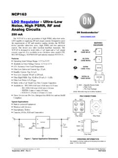
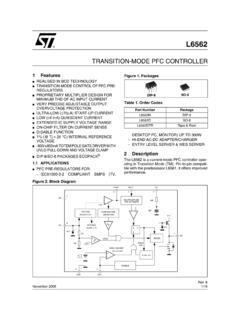
1 Low Dropout Regulator, Wide Input Voltage, Low Iq, 300 mA. NCP718 . The NCP718 is 300 mA LDO Linear Voltage Regulator. It is a very stable and accurate device with ultra low quiescent current consumption (typ. 4 mA over the full temperature range) and a wide Input voltage range (up to 24 V). The regulator incorporates several protection features such as Thermal Shutdown and Current Limiting. MARKING. DIAGRAMS. Features WDFN6 1. Operating Input Voltage Range: V to 24 V MT SUFFIX XX M. Fixed Voltage Options Available: V to 5 V (upon request) CASE 511BR. 1. Adjustable Voltage Option from V to 5 V XX = Specific Device Code Ultra Low Quiescent Current: typ. 4 mA over Temperature M = Date Code 2% Accuracy Over Full Load, Line and Temperature Variations TSOT 23 5. PSRR: 60 dB at 1 kHz SN SUFFIX XX MG. G. Noise: typ. 36 mVRMS from 100 Hz to 100 kHz 1 CASE 419AE. 1. Stable with Small 1 mF Ceramic Capacitor Soft start to Reduce Inrush Current and Overshoots XX = Specific Device Code M = Date Code*.
2 Thermal Shutdown and Current Limit Protection G = Pb Free Package SOA Limiting for High Vin / High Iout Static / Dynamic (Note: Microdot may be in either location). Active Discharge Option Available (upon request). *Date Code orientation and/or position may Available in TSOT 23 5 and WDFN6 2x2 mm Packages vary depending upon manufacturing location. These Devices are Pb Free, Halogen Free/BFR Free and are RoHS. Compliant PIN CONNECTIONS. Typical Applications Wireless Chargers OUT 1 6 IN. Portable Equipment NC/ADJ 2 GND 5 NC. Communication Systems GND 3 4 EN. V IN V OUT. IN OUT WDFN6 2x2 mm (Top View). NCP718 . 1 mF 1 mF. C IN C OUT. Ceramic EN GND NC Ceramic ON IN OUT. OFF. GND. Figure 1. Typical Application Schematic EN NC/ADJ. TSOT 23 5. (Top View). ORDERING INFORMATION. See detailed ordering and shipping information in the package dimensions section on page 7 of this data sheet. Semiconductor Components Industries, LLC, 2017 1 Publication Order Number: September, 2019 Rev. 9 NCP718 /D.
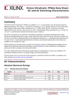
3 NCP718 . IN IN. ENABLE THERMAL ENABLE THERMAL. EN LOGIC SHUTDOWN EN LOGIC SHUTDOWN. BANDGAP BANDGAP. REFERENCE MOSFET REFERENCE MOSFET. INTEGRATED DRIVER WITH INTEGRATED DRIVER WITH. SOFT START CURRENT LIMIT SOFT START CURRENT LIMIT. OUT. OUT. ADJ. * ACTIVE DISCHARGE * ACTIVE DISCHARGE. Version A only Version A only EN EN. GND GND. Fixed Version Adjustable Version Figure 2. Simplified Block Diagram Table 1. PIN FUNCTION DESCRIPTION. Pin No. Pin No. (WDFN6) (TSOT 23 5) Pin Name Description 6 1 IN Input pin. A small capacitor is needed from this pin to ground to assure stability. 3, EXP 2 GND Power supply ground. 4 3 EN Enable pin. Driving this pin high turns on the regulator. Driving EN pin low puts the regulator into shutdown mode. 2 4 NC / ADJ Fixed Version: No connection. This pin can be tied to ground to improve thermal dissipation or left disconnected. Adjustable Version: Feedback pin for set up output voltage. Use resistor divider for voltage selection. 1 5 OUT Regulated output voltage pin.
4 A small 1 mF ceramic capacitor is needed from this pin to ground to assure stability. 5 N/C No connection. This pin can be tied to ground to improve thermal dissipation or left dis- connected. Table 2. ABSOLUTE MAXIMUM RATINGS. Rating Symbol Value Unit Input Voltage (Note 1) VIN to 24 V. Enable Voltage VEN to VIN+ V. Output Voltage VOUT to VIN+ (max. 6) V. Output Short Circuit Duration tSC Indefinite s Maximum Junction Temperature TJ(MAX) 150 C. Storage Temperature TSTG 55 to 150 C. ESD Capability, Human Body Model (Note 2) ESDHBM 2000 V. ESD Capability, Charged Device Model (Note 2) ESDCDM 1000 V. Stresses exceeding those listed in the Maximum Ratings table may damage the device. If any of these limits are exceeded, device functionality should not be assumed, damage may occur and reliability may be affected. 1. Refer to ELECTRICAL CHARACTERISTICS and APPLICATION INFORMATION for Safe Operating Area. 2. This device series incorporates ESD protection and is tested by the following methods: ESD Human Body Model tested per AEC Q100 002 (EIA/JESD22 A114).
5 ESD Charged Device Model tested per EIA/JESD22 C101, Field Induced Charge Model. Latch up Current Maximum Rating tested per JEDEC standard: JESD78. Latch up is not guaranteed on ENABLE pin. Table 3. THERMAL CHARACTERISTICS. Rating Symbol Value Unit Thermal Characteristics, WDFN6, 2 mm x 2 mm RqJA 65 C/W. Thermal Resistance, Junction to Air Thermal Characteristics, TSOT 23 5 RqJA 235 C/W. Thermal Resistance, Junction to Air 2. NCP718 . Table 4. ELECTRICAL CHARACTERISTICS -40 C TJ 125 C; VIN = V or (VOUT + V), whatever is greater; IOUT = 1 mA, CIN = COUT = 1 mF, unless otherwise noted. Typical values are at TJ = +25 C. (Note 3). Parameter Test Conditions Symbol Min Typ Max Unit Operating Input Voltage VIN 24 V. Output Voltage Accuracy 40 C TJ 125 C, VOUT < V VOUT 3% +3% V. (fixed versions) VOUT + 1 V < VIN < 16 V, mA < IOUT < 300 mA (Note 5) VOUT V 2% +2%. Reference Voltage 40 C TJ 125 C, VADJ V. VOUT + 1 V < VIN < 16 V. Reference Voltage Accuracy 40 C TJ 125 C, VOUT 2% +2% V. VOUT + 1 V < VIN < 16 V.
6 Line Regulation VOUT + 1 V VIN 16 V, Iout = 1 mA RegLINE 10 mV. Load Regulation IOUT = mA to 300 mA RegLOAD 10 mV. Dropout Voltage VDO = VIN (VOUT(NOM) 3%), V V VDO 480 mV. (Package TSOT 23 5) IOUT = 300 mA (Note 4). V V 320 490. V V 295 465. V V 275 440. 5V 250 380. Dropout Voltage VDO = VIN (VOUT(NOM) 3%), V V VDO 490 mV. (Package WDFN6) IOUT = 300 mA (Note 4). V V 335 505. V V 305 475. V V 285 450. 5V 260 395. Maximum Output Current VIN = VOUT + 1 V (Note 5) ILIM 300 800 mA. Disable Current VEN = 0 V, VIN = 5 V IDIS mA. Quiescent Current IOUT = 0 mA, 40 C TJ 125 C IQ mA. Ground current IOUT = 10 mA IGND 50 mA. IOUT = 300 mA 300. Power Supply Rejection Ratio VIN = V + 100 mVpp f = 1 kHz PSRR 60 dB. VOUT = V. IOUT = 1 mA, Cout = 1 mF. Output Noise Voltage VOUT = V, IOUT = 10 mA VN 36 mVrms f = 100 Hz to 100 kHz Enable Input Threshold Voltage Voltage increasing VEN_HI V. Voltage decreasing VEN_LO ADJ Pin Current VIN = VOUT + 1 V IADJ mA. EN Pin Current VEN = V IEN 100 nA. Active Output Discharge VIN = V, VEN = 0 V Rdis 100 W.
7 Resistance Thermal Shutdown Temperature Temperature increasing from TJ = +25 C TSD 165 C. (Note 6). Thermal Shutdown Hysteresis Temperature falling from TSD TSDH 25 C. (Note 6). Product parametric performance is indicated in the Electrical Characteristics for the listed test conditions, unless otherwise noted. Product performance may not be indicated by the Electrical Characteristics if operated under different conditions. 3. Performance guaranteed over the indicated operating temperature range by design and/or characterization production tested at TJ = TA =. 25 C. Low duty cycle pulse techniques are used during testing to maintain the junction temperature as close to ambient as possible. 4. Voltage Dropout for voltage variants below V is given by minimum Input voltage V. 5. Respect SOA. 6. Guaranteed by design and characterization. 3. NCP718 . TYPICAL CHARACTERISTICS. VIN = V. IQ, QUIESCENT CURRENT (mA). VOUT = V. VOUT, OUTPUT VOLTAGE (V). 125 C. CIN = 1 mF COUT = 1 mF. 25 C. IOUT = 1 mA 40 C.
8 VOUT = V. CIN = 1 mF. COUT = 1 mF. 40 20 0 20 40 60 80 100 120 2 4 6 8 10 12 14 16 18 20 22 24. TJ, JUNCTION TEMPERATURE ( C) VIN, Input VOLTAGE (V). Figure 3. Output Voltage vs. Temperature Figure 4. Quiescent Current vs. Input Voltage VOUT = V. CIN = 1 mF VEN = VIN. COUT = 1 mF. IDIS, DISABLE CURRENT (mA). IEN, ENABLE CURRENT (mA) VOUT = V. IOUT = 10 mA. CIN = 1 mF. COUT = 1 mF. VIN = 24 V VIN = 24 V. VIN = V VIN = V. 0 0. 40 20 0 20 40 60 80 100 120 40 20 0 20 40 60 80 100 120. TJ, JUNCTION TEMPERATURE ( C) TJ, JUNCTION TEMPERATURE ( C). Figure 5. Disable Current vs. Temperature Figure 6. Current to Enable Pin vs. Temperature 30 640. ISC, SHORT CIRCUIT CURRENT (mA). VIN = V VIN = V. 27 620. IGND, GROUND CURRENT (mA). VOUT = V VOUT = V. 24 CIN = 1 mF 600 CIN = 1 mF. 21 COUT = 1 mF 580 COUT = 1 mF. 18 560. 15 540. 12 520. 9 500. 6 480. 3 460. 0 440. 0 1 2 3 4 5 6 7 8 9 10 40 20 0 20 40 60 80 100 120. IOUT, OUTPUT CURRENT (mA) TJ, JUNCTION TEMPERATURE ( C). Figure 7. Ground Current vs.
9 Output Current Figure 8. Short Circuit Current vs. VOUT = V Temperature 4. NCP718 . TYPICAL CHARACTERISTICS. 600 VOUT = V. SOA CURRENT LIMITATION (mA). 540 125 C. VDROP, Dropout VOLTAGE (V). CIN = 1 mF. 480 COUT = 1 mF 25 C. 420 360 40 C. 300 240 180 f = 50 Hz Duty = 20%. 120 CIN = 1 mF 60 COUT = 1 mF 0 0. 0 2 4 6 8 10 12 14 16 18 20 22 24 0 VDIF, DIFFERENTIAL VOLTAGE VIN VOUT (V) IOUT, OUTPUT CURRENT (A). Figure 9. SOA Current Limit vs. Differential Figure 10. Dropout Voltage vs. Output Current Voltage VOUT = V. 90 90. 1 mA. 80 80. RR, RIPPLE REJECTION (dB). RR, RIPPLE REJECTION (dB). 1 mA. 70 70 10 mA. 60 10 mA 60. 50 50. 40 40 100 mA. VIN = V VIN = 12 V. 30 30. VOUT = V VOUT = V. 100 mA. 20 CIN = 1 mF 20 CIN = 1 mF. COUT = 1 mF COUT = 1 mF. 10 MLCC, X7R, 0805 10 MLCC, X7R, 0805. 0 0. 10 100 1K 10K 100K 1M 10M 10 100 1K 10K 100K 1M 10M. FREQUENCY (Hz) FREQUENCY (Hz). Figure 11. Power Supply Rejection Ratio vs. Figure 12. Power Supply Rejection Ratio vs. Current, VIN = V, COUT = 1 mF Current, VIN = 12 V, COUT = 1 mF.
10 100K 100K. OUTPUT VOLTAGE NOISE (nV/ Hz). OUTPUT VOLTAGE NOISE (nV/ Hz). 10K 10K. 1K 1K. VIN = V VIN = V. VOUT = V VOUT = V. IOUT = 10 mA IOUT = 10 mA. 100 100 CIN = 1 mF. CIN = 1 mF. COUT = 1 mF COUT = 1 mF. MLCC, X7R, 0805 MLCC, X7R, 0805. 10 10. 10 100 1K 10K 100K 1M 10 100 1K 10K 100K 1M. FREQUENCY (Hz) FREQUENCY (Hz). Figure 13. Output Voltage Noise Spectral Figure 14. Output Voltage Noise Spectral Density for VOUT = V, IOUT = 10 mA, Density for VOUT = V, IOUT = 10 mA, COUT = 1 mF COUT = 1 mF. 5. NCP718 . APPLICATIONS INFORMATION. The NCP718 is the member of new family of Wide Input The maximum power dissipation the NCP718 can handle Voltage Range Low Dropout Regulators which delivers is given by: Ultra Low Ground Current consumption, Good Noise and Power Supply Rejection Ratio Performance. The NCP718 . TJ(MAX) * TA . P D(MAX) + (eq. 1). incorporates EN pin and soft start feature for simple R qJA. controlling by microprocessor or logic. The power dissipated by the NCP718 for given application conditions can be calculated from the following Input Decoupling (CIN).