Transcription of New High Current MOSFET Module Offers 177 µΩ RDS(on)
1 New high Current MOSFET Module Offers 177 RDS(on) By William C. Kephart, Eric R. Motto Application Engineering Powerex Incorporated Abstract This paper describes a new family of high Current MOSFET modules optimized for industrial electric vehicle applications. While the MOSFET Module is configured as a six pack for an inverter topology, the MOSFET Module can easily be converted to a high Current dual or chopper for use in other topologies. Each element in the Module consists of a single large area chip providing excellent avalanche characteristics and ultra low RDS(on).
2 Chopper operation is further enhanced via reduced static losses in the free wheel diode by utilizing the reverse conduction characteristics of the MOSFET element. Introduction mosfets enjoy widespread use in low voltage power topologies such as inverters and choppers due to their low conduction losses, low switching losses, high frequency operation capability, inherent free wheeling diode and avalanche capability. These characteristics combine to create an efficient, robust power circuit. high Current operation requires paralleling several discrete mosfets . While operating mosfets in parallel is relatively easy, this mode of packaging has several disadvantages: (1) Complex assembly requiring many components including the mosfets , a low inductance bus system, gate signal routing, electrical insulation system and heat removal system, (2) Low avalanche capability generally limited to the avalanche capability of one of the paralleled mosfets , (3) Reduced reliability due to the large number of components utilized.
3 (4) Large area needed for the assembly. In order to address the disadvantages of high Current MOSFET applications, a new series of MOSFET modules has been introduced. This family of MOSFET modules are configured in a six pack (basic inverter topology) using a single large area element for each switch. The large area element concept results in a high avalanche capability and very low on resistance (RDS(on)). The Module is an isolated base type giving the designer all the advantages of the familiar higher voltage IGBT Module with regard to system packaging. Because of the common isolated base plate the inverter legs can be easily paralleled by simply connecting the output terminals together creating a dual with three times the Current carrying capability of a single inverter leg.
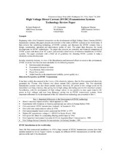
4 Creating a chopper Module is easy by shorting the gates of upper mosfets . New high Current MOSFET Module Offers 177 RDS(on) By William C. Kephart and Eric R. Motto MOSFET Module Structure The MOSFET Family consists of 200 ampere, 400 ampere and 600 ampere Current rated modules at 75 volts, 100 volts and 150 volts. The entire family of modules shares the same package shown in figure 1. The Module schematic is shown in figure 2. The MOSFET Module is housed in the U series high power type package utilizing the flow through configuration with bus connections one side and the three output terminals on the other side.
5 The U series package is designed to minimize internal inductance [1]. A high reliability automotive type connector is used for the gate connections and the internal temperature sensor. The copper base plate combined with the large area element combine to deliver a low thermal resistance ( C/W per element measured under the element for the 600A Module ). The large area element results in a very low RDS(on), as low as 177 for the 75V, 600A Module connected as a dual. In the six pack inverter configuration RDS(on) is 531 resulting in just Watts conduction loss per element for an inverter supplying 150 amperes(RMS) output from a 48V bus and a switching frequency of 10 KHz.
6 The MOSFET Module approach to low voltage, high Current applications Offers the designer a much better packaging solution than a paralleled discrete MOSFET package solution. As an example, consider a 600A inverter circuit. With discrete 60 ampere mosfets in TO247AD packages, a total of 60 mosfets would be required assuming perfect sharing along with the necessary substrate or bus, interconnecting means, gate signal wiring, electrical isolation and thermal system. Sixty TO247AD package yields a footprint of 19,200mm2 as compared to the MOSFET Module footprint of 9,900mm2 The discrete approach has almost twice the footprint as the MOSFET Module .
7 Figure 1: MOSFET Module Package Figure 2: MOSFET Module Schematic New high Current MOSFET Module Offers 177 RDS(on) By William C. Kephart and Eric R. Motto Temperature Sensing One of the useful features of the MOSFET family that is needed in most if not all power electronic applications is the ability to sense temperature. In most power electronic systems temperature is typically monitored using a sensor mounted on the same heatsink as the power semiconductor Module . The difficulty with this approach is that the temperature sensor is a significant distance from the source of heat generation, namely the MOSFET elements.
8 In order to properly protect the MOSFET elements from experiencing an over temperature event the designer needs to know the worst case losses in the circuit and thermal impedances between the elements and the temperature sensor location so that perfect coordination exists between temperature sensor and the MOSFET elements[2]. Further, the designer must understand the complex relationships existing between these factors to protect the MOSFET elements from premature or catastrophic failure. The designer may opt to use a large safety factor in selecting the sensor to compensate for careful analysis resulting in under utilization of MOSFET capability.
9 The MOSFET Module incorporates an integrated sensor within the Module . By building in the temperature sensor many of the issues described above are eliminated and effective thermal protection of the Module is achieved. Access to the internal thermistor allows accurate temperature monitoring for precise over temperature protection. Figure 3 shows the relationship between the thermistor s resistance and the Case Temperature. Figure 3: Thermistor Characteristic New high Current MOSFET Module Offers 177 RDS(on) By William C. Kephart and Eric R. Motto Reverse Conduction Mode One advantage of a MOSFET is its ability to act as a diode when reversed biased.
10 This diode action functions as the device Free Wheel diode (FWD) common in voltage source inverter circuits. As with conventional FWDs, losses are incurred when Current is flowing it the diode. In a typical induction motor drive, the conduction losses in FWD is in the range of 7% to 12% of the total losses for the switch depending on load power factor. For a chopper application, however, the chopper diode conduction loss can represent more than half the total losses. The MOSFET Module can easily be converted to a chopper Module simply be shorting the gate to source on upper MOSFET allowing it to always act as a diode (see Figure 4).