Transcription of NJM4580 - New Japan Radio Co.,Ltd.( New JRC )
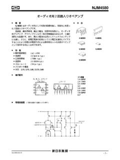
1 DUAL OPERATIONAL AMPLIFIER GENERAL DESCRIPTION PACKAGE OUTLINE The NJM4580 is a dual operational amplifier, specially designed for improving the tone control, which is most suitable for the audio application. Featuring noiseless, higher gain bandwidth, high output current and low distortion ratio, and it is most suitable not only for acoustic electronic parts of audio pre-amp and active filter, but also for the industrial measurement tools. It is also suitable for the head phone amp at higher output current, and further more, it can be applied for the handy type set operational amplifier of general purpose in application of low voltage single supply type which is properly biased of the low voltage source.
2 The D-Rank type products(NJM4580DD/LD/MD/ED) have specified maximum limits for equivalent input noise voltage. FEATURES Operating Voltage 2V~ 18V Low Input Noise Voltage Vrms typ. (RIAA) Wide GBW 15 MHz typ. Low Distortion typ. Slew Rate 5V/ s typ. Bipolar Technology Package Outline DIP8, SIP8, DMP8, SSOP8, MSOP8(VSP8) MEET JEDEC MO-187-DA SOP8 JEDEC 150mil PIN CONFIGURATION EQUIVALENT CIRCUIT ( 1/2 Shown ) NJM4580D ( DIP8 ) NJM4580L( SIP8 ) NJM4580E ( SOP8 ) NJM4580M( DMP8 ) NJM4580R (MSOP8(VSP8 )) NJM4580V( SSOP8 ) -INPUT+INPUTV+V-OUTPUT PIN FUNCTION1. A OUTPUT 2. A - INPUT 3. A +INPUT 4. V- 5. B +INPUT 6. B - INPUT 7. B OUTPUT 8. V+ 87651234AB( Top View )NJM4580D, NJM4580M, NJM4580E NJM4580V, NJM4580R AB1 234567 8 NJM4580L NJM4580 ABSOLUTE MAXIMUM RATINGS (Ta=25 C, unless otherwise noted.)
3 PARAMETER SYMBOLRATING UNIT Supply Voltage V+/V- 18 V Input Voltage VICM 15 (Note1) V Differential Input Voltage VID 30 (Note1) V Power Dissipation PD DIP8, SIP8 : 800 DMP8, SOP8 : 300 SSOP8 : 250 MSOP8(VSP8) : 400 (Note2) mW Operating Temperature Range Topr -40~+85 C Storage Temperature Range Tstg -40~+125 C (Note1) For supply voltage less than 15V, the absolute maximum input voltage is equal to supply voltage.
4 (Note2) On the PCB "EIA/JEDEC ( , 2 layers, FR-4)" RECOMMENDED OPERATING CONDITIONS (Ta=25 C) PARAMETER SYMBOLCONDITION MIN. TYP. Voltage V+/V- 2 - 18 V ELECTRICAL CHARACTERISTICS (V+/V-= 15V, Ta=25 C, unless otherwise noted.) PARAMETER SYMBOLTEST CONDITION MIN. TYP. Offset Voltage VIO RS 10k - 3 mV Input Offset Current IIO - 5 200 nA Input Bias Current IB - 100 500 nA Voltage Gain AV RL 2k.
5 VO= 10V 90 110 - dB Maximum Output Voltage VOM RL 2k 12 - V Common Mode Input Voltage Range VICM 12 - V Common Mode Rejection Ratio CMR RS 10k 80 110 - dB Supply Voltage Rejection Ratio SVR RS 10k 80 110 - dB Supply Current ICC - 6 9 mA Slew Rate SR RL 2k - 5 - V/ s Gain Bandwidth Product GB f=10kHz - 15 - MHz Total Harmonic Distortion THD AV=20dB,VO=5V,RL=2k.
6 F=1kHz - - % Equivalent Input Noise Voltage VNI RIAA,RS= ,30kHz LPF - - Vrms ELECTRICAL CHARACTERISTICS (D-rank type(Note3), V+/V-= 15V, Ta=25 C, unless otherwise noted.) PARAMETER SYMBOLTEST CONDITION MIN. TYP. Input Noise Voltage VNI RIAA,RS= - - Vrms(Note3)D-rank type is a Equivalent Input Noise Voltage selected product. It s only DIP, DMP, SOP and SIP package. TYPICAL CHARACTERISTICS Maximum Output Voltage vs.
7 FrequencyV+/V-= 15V, RL=2k , Ta=25 C0510152025301k10k100k1M10 MFrequency [Hz]Maximum Output Voltage [VPP]Maximum Output Voltage vs. Output CurrentV+/V-= 15V, Ta=25 C-15-10-5051015110100 Output Current [mA]Maximum Output Voltage [V]+VOM-VOMTHD vs. Output Voltage (Frequency)V+/V-= 15V, GV=20dB, RL=2k Voltage [Vrms]THD+N [%]f=20kHzf=1kHzf=20Hz40dB Gain/Phase vs. Frequency(V+/V-= 15V, RL=2k , Ta=25 C)051015202530354045501k10k100k1M10 MFrequency [Hz]Voltage Gain [dB]-180-150-120-90-60-300 Phase [deg]GainPhaseMaximum Output Voltage vs. Load ResistanceV+/V-= 15V, Ta=25 C-15-10-50510151001k10kLoad Resistance [ ]Maximum Output Voltage [V]+VOM-VOMV oltage Noisevs. FrequencyV+/V-= 15V, RS=50 , GV=60dB, Ta=25 C051015201101001kFrequency [Hz]Equivalent Input Noise Voltage[nV/ Hz] NJM4580 TYPICAL CHARACTERISTICS Maximum Output Voltage vs.
8 TemperatureV+/V-= 15V, RL=2k -15-10-5051015-50-250255075100125 Ambient Temperature [ C]Maximum Output Voltage [V]+VOM-VOMI nput Offset Voltage vs. TemperatureV+/V-= Temperature [ C]Input Offset Voltage [mV]Input Bias Current vs. TemperatureV+/V-= 15V050100150200250300350400450-50-250255 075100125 Ambient Temperature [ C]Input Bias Current [nA]Supply Current vs. Supply VoltageTa=25 C012345670 2 4 6 8 10 12 14 16 18 Supply Voltage V+/V- [V]Supply Current [mA]Supply Current vs. TemperatureV+/V-= 15V024681012-50-250255075100125 Ambient Temperature [ C]Supply Current [mA]Maximum Output Voltage vs. Supply VoltageRL=2k , Ta=25 C-18-12-60612180 2 4 6 8 10 12 14 16 18 Supply Voltage V+/V- [V]Maximum Output Voltage [V]+VOM-VOM TEST CIRCUIT 47 100 100 -15V+ 220k40dB Amp30kHz LPFVoutNoise Voltage (RIAA) measurement circuit [CAUTION] The specifications on this databook are only given for information , without any guarantee as regards either mistakes or omissions.
9 The application circuits in this databook are described only to show representative usages of the product and not intended for the guarantee or permission of any right including the industrial rights.