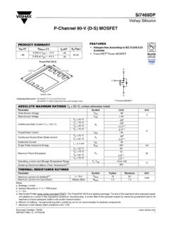
Transcription of P-Channel 40 V (D-S) MOSFET - Vishay Intertechnology
1 Vishay SiliconixSi2319 CDSD ocument Number: 66709S10-1286-Rev. A, 40 V (D-S) MOSFETFEATURES Halogen-free According to IEC 61249-2-21 Definition TrenchFET Power MOSFET 100 % Rg Tested Compliant to RoHS Directive 2002/95/ECAPPLICATIONS Load Switch DC/DC ConverterNotes:a. Based on TC = 25 Surface mounted on 1" x 1" FR4 t = 5 s. d. Maximum under steady state conditions is 166 SUMMARY VDS (V)RDS(on) ( )ID (A)aQg (Typ.)- at VGS = - 10 V - at VGS = - V - (SOT-23)SDTo p View231Si2319 CDS (P7)** Marking CodeOrdering Information.
2 Si2319 CDS-T1-GE3 (Lead (Pb)-free and Halogen-free)SGDP- channel MOSFET ABSOLUTE MAXIMUM RATINGS TA = 25 C, unless otherwise notedParameter Symbol Limit Unit Drain-Source Voltage VDS- 40 VGate-Source Voltage VGS 20 Continuous Drain Current (TJ = 150 C)
3 TC = 25 CID- = 70 C- = 25 C- , cTA = 70 C- , cPulsed Drain CurrentIDM- 20 Continous Source-Drain Diode CurrentTC = 25 CIS- = 25 C- 1b, cMaximum Power DissipationTC = 25 = 70 = 25 , cTA = 70 , cOperating Junction and Storage Temperature RangeTJ, Tstg - 55 to 150 CTHERMAL RESISTANCE RATINGS Parameter Symbol TypicalMaximumUnit Maximum Junction-to-Ambientb, dt 5 sRthJA75100 C/WMaximum Junction-to-Foot (Drain)Steady Number: 66709S10-1286-Rev.
4 A, 31-May-10 Vishay SiliconixSi2319 CDSN otes:a. Pulse test; pulse width 300 s, duty cycle 2 %.b. Guaranteed by design, not subject to production testing. Stresses beyond those listed under Absolute Maximum Ratings may cause permanent damage to the device. These are stress ratings only, and functional operationof the device at these or any other conditions beyond those indicated in the operational sections of the specifications is not implied. Exposure to absolute maximumrating conditions for extended periods may affect device TJ = 25 C, unless otherwise notedParameter Symbol Test Conditions Min.
5 StaticDrain-Source Breakdown VoltageVDS VGS = 0 V, ID = - 250 A - 40 VVDS Temperature Coefficient VDS/TJID = - 250 A - 40mV/ CVGS(th) Temperature Coefficient VGS(th) Threshold VoltageVGS(th)VDS = VGS , ID = - 250 A - LeakageIGSSVDS = 0 V, VGS = 20 V 100nAZero Gate Voltage Drain CurrentIDSSVDS = - 40 V, VGS = 0 V- 1 AVDS = - 40 V, VGS = 0 V, TJ = 55 C - 5On-State Drain CurrentaID(on) VDS - 5 V, VGS = - 10 V - 20 ADrain-Source On-State ResistanceaRDS(on)VGS = - 10 V, ID = - A VGS = - V, ID = - A TransconductanceagfsVDS = - 15 V, ID = - A 10 SDynamicbInput CapacitanceCiss VDS = - 20 V, VGS = 0 V, f = 1 MHz595pFOutput CapacitanceCoss 76 Reverse Transfer CapacitanceCrss 61 Total Gate ChargeQg VDS = - 20 V, VGS = - 10 V, ID = - = - 20 V, VGS = - V, ID = - A711 Gate-Source ChargeQgs ResistanceRgf = 1 Tu r n - O n D e l a y T i m etd(on)
6 VDD = - 20 V, RL = 8 ID - A, VGEN = - V, Rg = 1 4060nsRise Timetr 2741 Turn-Off Delay Timetd(off) 1827 Fall Timetf1020Tu r n - O n D e l a y T i m etd(on) VDD = - 20 V, RL = 8 ID - A, VGEN = - 10 V, Rg = 1 816 Rise Timetr 918 Turn-Off Delay Timetd(off) 2030 Fall Timetf816 Drain-Source Body Diode CharacteristicsContinuous Source-Drain Diode CurrentISTC = 25 C- Diode Forward CurrentISM- 20 Body Diode VoltageVSDIS = - A, VGS = 0 V- Diode Reverse Recovery TimetrrIF = - A, dI/dt = 100 A/ s, TJ = 25 C1726nsBody Diode Reverse Recovery ChargeQrr918nCReverse Recovery Fall Timeta10nsReverse Recovery Rise Timetb7 Document Number: 66709S10-1286-Rev.
7 A, SiliconixSi2319 CDSTYPICAL CHARACTERISTICS 25 C, unless otherwise notedOutput CharacteristicsOn-Resistance vs. Drain CurrentGate - Drain-to-Source Voltage (V)ID - Drain Current (A) - 10 VVGS= - VRDS(on) - On-Resistance ( )ID - Drain Current (A)024681003691215ID= - Total Gate Charge (nC)VGS - Gate-to-Source Voltage (V)Transfer CharacteristicsCapacitanceOn-Resistance vs. Junction Temperature01234501234TC= 25 CTC= 125 CTC= - 55 CVGS - Gate-to-Source Voltage (V)ID - Drain Current (A)025050075010000816243240 CissCossCrssVDS - Drain-to-Source Voltage (V)C - Capacitance (pF) 50- 250255075100125150 VGS= ;ID= - 10 V; ID= - Junction Temperature ( C)(Normalized)RDS(on) - Number: 66709S10-1286-Rev.
8 A, 31-May-10 Vishay SiliconixSi2319 CDSTYPICAL CHARACTERISTICS 25 C, unless otherwise notedSource-Drain Diode Forward VoltageThreshold - Source-to-Drain Voltage (V)IS - Source Current (A)TJ=25 CTJ= 150 50- 250255075100125150ID= - 250 AVGS(th) (V)TJ - Temperature ( C)On-Resistance vs. Gate-to-Source VoltageSingle Pulse Power (Junction-to-Ambient) CTJ= 125 CID= (on) - On-Resistance ( )VGS - Gate-to-Source Voltage (V) (s)Power (W)TA= 25 CSafe Operating Area, CSingle Pulse1s,10sLimited by RDS(on)*BVDSS Limited1ms100 s10 msDC100 msVDS - Drain-to-Source Voltage (V)* VGS > minimum VGS at which RDS(on) is specifiedID - Drain Current (A)Document Number: 66709S10-1286-Rev.
9 A, SiliconixSi2319 CDSTYPICAL CHARACTERISTICS 25 C, unless otherwise noted* The power dissipation PD is based on TJ(max) = 150 C, using junction-to-case thermal resistance, and is more useful in settling the upperdissipation limit for cases where additional heatsinking is used. It is used to determine the current rating, when this rating falls below the Derating*0123450255075100125150TC - Case Temperature ( C)ID - Drain Current (A)Power, - Case Temperature ( C)Power (W)Power, - Ambient Temperature ( C)Power (W) Number: 66709S10-1286-Rev.
10 A, 31-May-10 Vishay SiliconixSi2319 CDSTYPICAL CHARACTERISTICS 25 C, unless otherwise notedVishay Siliconix maintains worldwide manufacturing capability. Products may be manufactured at one of several qualified locations. Reliability data for SiliconTechnology and Package Reliability represent a composite of all qualified locations. For related documents such as package/tape drawings, part marking, andreliability data, see Thermal Transient Impedance, Duration (s)Normalized Effective TransientThermal :PDM1.