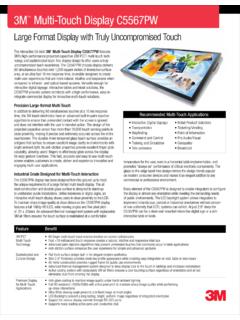
Transcription of PCTS for Metal Mesh - Bison (ENG) - gredmann.com
1 1~~~~~~~~~~~~~~~~ Metal Mesh Touch SensorMetal Mesh Touch SensorMetal Mesh Touch SensorMetal Mesh Touch Sensor~~~~~~~~~~~~~~~~ Bison Copper Mesh Bison Copper Mesh Bison Copper Mesh Bison Copper Mesh The way of TP The way of TP The way of TP The way of TP revolution, revolution, revolution, revolution, we drive it ! we drive it ! we drive it ! we drive it ! HWL HWL HWL HWL (((( Metal Mesh 42 Metal Mesh 42 Metal Mesh 42 Metal Mesh TTTT ouch ouch ouch ouch PPPP anelanelanelanelResearch Motivation Research Motivation Research Motivation Research Motivation Motivation:1. Considering the price of ITO film, capacitive TP above 15 is no Size above 15 , film sensor resistive is too high to design. Double routing will cause the BM Size above 15 , IC resistive will increase route numbers in route area. Route width needs to be 30um / Metal Mesh is developed to replace ITO by Fuji film, Panasonic, 3M and :Using copper-etching process can replace ITO, solve the design issue and develop Metal Mesh.))))
2 Also, we can use its price advantage to compete with other companies in US and Mesh Advantage Metal Mesh Advantage Metal Mesh Advantage Metal Mesh Advantage Metal Mesh Advantage:1. If choosing Metal route to replace ITO, the cost of film sensor can be cost-down 30%. Especially for the TP size above 15 .2. Etching process can make traces and Metal Mesh at one time. The process is short and the cost is Resistive is low, so double routing is not necessary. The design can be simple. Etching process can achieve thin traces, and BM will be very thin as Resistive is low, so 70 is According to the low resistive, The TP sensitivity is better. Touch signal and anti-interference are better than ITO Sensor!~~ Metal Mesh ~~ Metal Mesh ~~ Metal Mesh ~~ Metal Mesh Projected capacitive Touchscreen~~~~~~~~Function ConfirmedFunction ConfirmedFunction ConfirmedFunction ConfirmedBlack Treatment Copper Conductive Film (Copper (Cu) Mesh)Transparent Conductive Film Touch Panel (Copper (Cu) Mesh) Metal Mesh ProcessMetal Mesh ProcessMetal Mesh ProcessMetal Mesh Process Cu-SputteringBlack OxideEtchingSheetLaminationSheet LaserBonding FPCC over LaminationDegassingAppearance inspectionFunction checkShipmentMetal Mesh PCAP TP Structure Metal Mesh PCAP TP Structure Metal Mesh PCAP TP Structure Metal Mesh PCAP TP Structure Cover GlassOCAFilmFilmOCAT echnical Capacity:1.
3 Photo Image etch(Active Area): Copper Linewidth/Line Pitch : 3~6um /200um~600um2. Photo Image etch(Border Area): Copper Linewidth/Line Space : 30um /30umCopper Black Copper Black Copper Black Copper Black TreatmentTreatmentTreatmentTreatmentPETC uBTCuBTCuBTBT: Black TreatmentBlack TreatmentBlack Treatment: 1. Anti-Oxidize2. Anti-Reflection3. Enhance TransmittancePCAP TP StructurePCAP TP StructurePCAP TP StructurePCAP TP Structure20132015 GFF (Copper Mesh 15um~25um )GFF (Copper Mesh 5um~7um )GFF (Black Treatment Copper Mesh 5um~7um )GF2 (Black Treatment Copper 5um~7um)GF2 (Black Treatment Copper 3um~5um)2014 Metal Mesh Develop for InvisibilityGFF (Black Treatment Copper Mesh 3um~5um )PETCuBTCuBTCuBTBT: Black TreatmentPETCuCuCuPETCuBTCuBTCuBTBT: Black TreatmentCuBTCuBTConcern Concern Concern Concern and Solution for and Solution for and Solution for and Solution for Metal MeshMetal MeshMetal MeshMetal MeshMetal Mesh Improves Optical Issues:1. Optical features: Optical issues can be solved by process ability.
4 Light transmittance and haze are similar to film Moire effect can be avoided via Pattern Visible: Making thin trace (5 2um, mask improving can achieve 3um) via etching Process can solve this Concern Concern Concern aaaand Solution for nd Solution for nd Solution for nd Solution for MoireMoireMoireMoire Pattern Pattern Pattern Pattern 1. Moire Pattern: Overlapping Palisade fringes cause the interference Metal Mesh is full of untransparent traces. The traces overlap with the LCD color filter can cause interference images as the upper right to improve: Random pattern design can improve this issue. We have conquered this problem!Moire Pattern - BeforeMoire Pattern - AfterSpecification Specification Specification Specification for for for for GredmannGredmannGredmannGredmann Copper Mesh Copper Mesh Copper Mesh Copper Mesh ItemGFF TypeGF2 TypeCu Film StructureLine Width (Active Area) 5um 5umLine Space (Border Area): Min. 15um/15umMin. 30um/30umMesh ~ ~1mmTransmittance< 90% < 90%Haze< 2%<2%MoireMoire FreeMoire FreeSheet Resistance(before Patterning)< / < / Film Sensor ~ (With OCA) (With OCA)PETCuBTCuBTCuBTBT: Black TreatmentPETCuBTCuBTCuBTBT: Black TreatmentCuBTCuBTSpecification for Specification for Specification for Specification for GredmannGredmannGredmannGredmann Copper Mesh Copper Mesh Copper Mesh Copper Mesh ItemElectrode FormationLine Width(um)Sheet Resistance( )TP Max.
5 Size (in)Transmittance/Haze(%)Tracing ProcessITO Film /ITO GlassPrinting Resist /Etching TransparenceFilm:150 Glass:602088%/ 2%Another ProcessPrinting Mesh(Korea TP Company)Ag PastePrinting10~ by Sensor Patterning (One Process)Ag nano Wiring(TPK&Cambrios /Carestream)EtchTransparence(Ag Haze)60~1002088%/5%Another ProcessAg-halide Wiring(Fuji Film)Photographic5~10502088%/2%Make by Sensor Patterning (One Process) Bison Copper MeshPhoto imageEtcging5~ by Sensor Patterning (One Process)Our Business ModelOur Business ModelOur Business ModelOur Business ModelModel I : Mesh TP Module MaterialPattern DesignEtchingFF LaminationCover LaminationModel II: Mesh FF SensorMaterialPattern DesignEtching FF LaminationModel III: Mesh FilmMaterialPattern DesignEtching CustomerCustomerCustomerCustomerControll er Connection and Adjustment16 Thank you !