Transcription of PD - 95810 IRFP1405 - Infineon Technologies
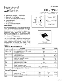
1 HEXFET Power MOSFETVDSS = 55 VRDS(on) = ID = MOSFETPD - 95810 Specifically designed for Automotive applications, this HEXFET Power MOSFET utilizes the latest processing techniques toachieve extremely low on-resistance per silicon area. Additionalfeatures of this design are a 175 C junction operating tempera-ture, fast switching speed and improved repetitive avalancherating . These features combine to make this design an extremelyefficient and reliable device for use in Automotive applications anda wide variety of other Advanced Process Technology Ultra Low On-Resistance 175 C Operating Temperature Fast Switching Repetitive Avalanche Allowed up to TjmaxFeaturesHEXFET is a registered trademark of International Rectifier.
2 *2 2 2 2 2 t2 22WH gIRFP1405TO-247AC hqAbsolute Maximum RatingsParameterUnitsID @ TC = 25 CContinuous Drain Current, VGS @ 10V (Silicon Limited)ID @ TC = 100 CContinuous Drain Current, VGS @ 10V AID @ TC = 25 CContinuous Drain Current, VGS @ 10V (Package Limited)IDMP ulsed Drain Current cPD @TC = 25 CPower Dissipation WLinear Derating Factor W/ CVGSGate-to-Source VoltageVEAS (Thermally limited) Single Pulse Avalanche EnergydmJEAS (Tested ) Single Pulse Avalanche Energy Tested Value hIARA valanche Current cAEARR epetitive Avalanche Energy gmJTJ Operating Junction andTSTGS torage Temperature Range CSoldering Temperature, for 10 secondsMounting Torque, 6-32 or M3 screwThermal JC Junction-to-Case * cs Case-to-Sink, Flat, Greased Surface C/WR JA Junction-to-Ambient * 401060530 See , 12b, 15, to + 175300 ( from case )10 lbfyin ( )s p Characteristics @ TJ = 25 C (unless otherwise specified)ParameterMin.
3 Typ. Max. UnitsV(BR)DSSD rain-to-Source Breakdown Voltage55 V V(BR)DSS/ TJ Breakdown Voltage Temp. Coefficient V/ CRDS(on)Static Drain-to-Source On-Resistance VGS(th)Gate Threshold Transconductance77 SIDSSD rain-to-Source Leakage Current 20 A 250 IGSSGate-to-Source Forward Leakage 200nAGate-to-Source Reverse Leakage -200 QgTotal Gate Charge 120180 QgsGate-to-Source Charge 30 nCQgdGate-to-Drain ("Miller") Charge 53 td(on)Turn-On Delay Time 12 trRise Time 160 td(off)Turn-Off Delay Time 140 nstfFall Time 150 LDInternal Drain Inductance Between lead, nH6mm ( )
4 LSInternal Source Inductance 13 from packageand center of die contactCissInput Capacitance 5600 CossOutput Capacitance 1310 CrssReverse Transfer Capacitance 350 pFCossOutput Capacitance 6550 CossOutput Capacitance 920 Coss Output Capacitance 1750 Source-Drain Ratings and Characteristics ParameterMin. Typ. Max. UnitsISContinuous Source Current 95(Body Diode)AISMP ulsed Source Current 640(Body Diode) cVSDD iode Forward Voltage Recovery Time 70110nsQrrReverse Recovery Charge 170260nCtonForward Turn-On TimeIntrinsic turn-on time is negligible (turn-on is dominated by LS+LD)
5 VGS = 0V, VDS = , = = 0V, VDS = 44V, = = 0V, VDS = 0V to 44V fVGS = 10V eVDD = 28 VID = 95 ARG = TJ = 25 C, IS = 95A, VGS = 0V eTJ = 25 C, IF = 95A, VDD = 28 Vdi/dt = 100A/ s eConditionsVGS = 0V, ID = 250 AReference to 25 C, ID = 1mA VGS = 10V, ID = 95A eVDS = VGS, ID = 250 AVDS = 55V, VGS = 0 VVDS = 55V, VGS = 0V, TJ = 125 CMOSFET symbolshowing theintegral reversep-n junction = 25V, ID = 95 AID = 95 AVDS = 44 VConditionsVGS = 10V eVGS = 0 VVDS = 25V = = 20 VVGS = -20V 2 Repetitive rating; pulse width limited by max. junction temperature. (See fig. 11). 2 Limited by TJmax, starting TJ = 25 C, L = RG = 25 , IAS = 95A, VGS =10V.
6 Part not recommended for use above this value. Pulse width ; duty cycle 2%.x X Coss eff. is a fixed capacitance that gives the same charging time as Coss while VDS is rising from 0 to 80% VDSS . 2 Limited by TJmax , see , 12b, 15, 16 for typical repetitive avalanche performance. 2 This value determined from sample failure population. 100% tested to this value in p 2. Typical Output CharacteristicsFig 1. Typical Output CharacteristicsFig 3. Typical Transfer CharacteristicsFig 4. Typical Forward TransconductanceVs. Drain , Drain-to-Source Voltage (V)101001000ID, Drain-to-Source Current (A) 60 s PULSE WIDTHTj = 175 , Gate-to-Source Voltage (V)101001000ID, Drain-to-Source Current ( )VDS = 25V 60 s PULSE WIDTHTJ = 25 CTJ = 175 , Drain-to-Source Voltage (V)1101001000ID, Drain-to-Source Current (A) 60 s PULSE WIDTHTj = 25 20406080100ID, Drain-to-Source Current (A)020406080100120140 Gfs, Forward Transconductance (S)TJ = 25 CTJ = 175 CVDS = 10V380 s PULSE WIDTHs p 8.
7 Maximum Safe Operating AreaFig 6. Typical Gate Charge VoltageFig 5. Typical Capacitance VoltageFig 7. Typical Source-Drain DiodeForward Voltage110100 VDS, Drain-to-Source Voltage (V)0200040006000800010000C, Capacitance (pF)CossCrssCissVGS = 0V, f = 1 MHZCiss = Cgs + Cgd, Cds SHORTEDCrss = Cgd Coss = Cds + Cgd04080120160200 QG Total Gate Charge (nC)048121620 VGS, Gate-to-Source Voltage (V)VDS= 44 VVDS= 28 VID= 95 AFOR TEST CIRCUITSEE FIGURE , Source-toDrain Voltage (V) , Reverse Drain Current (A)TJ = 25 CTJ = 175 CVGS = 0V1101001000 VDS , Drain-toSource Voltage (V) , Drain-to-Source Current (A)Tc = 25 CTj = 175 CSingle Pulse1msec10msecOPERATION IN THIS AREA LIMITED BY RDS(on)100 secDCs p 11.
8 Maximum Effective Transient Thermal Impedance, Junction-to-CaseFig 9. Maximum Drain Current TemperatureFig 10. Normalized On-ResistanceVs. Temperature255075100125150175 TC , Case Temperature ( C)050100150200ID , Drain Current (A)LIMITED BY PACKAGE-60-40-20020406080100120140160180 TJ , Junction Temperature ( C) (on) , Drain-to-Source On Resistance (Normalized)ID = 95 AVGS = , Rectangular Pulse Duration (sec) Response ( Z thJC ) = PULSE( THERMAL RESPONSE )Notes:1. Duty Factor D = t1/t22. Peak Tj = P dm x Zthjc + TcRi ( C/W) i (sec) J J 1 1 2 2R1R1R2R2 CCii/RiCi= i/Ris p Fig 13b.
9 Gate Charge Test CircuitFig 13a. Basic Gate Charge WaveformFig 12c. Maximum Avalanche EnergyVs. Drain CurrentFig 12b. Unclamped Inductive WaveformsFig 12a. Unclamped Inductive Test CircuittpV(BR)DSSIASFig 14. Threshold Voltage Vs. +-VDDDRIVERA15V20 VVGS255075100125150175 Starting TJ, Junction Temperature ( C)0500100015002000 EAS, Single Pulse Avalanche Energy (mJ) IDTOP 16A 20 ABOTTOM 95A-75-50-250255075100125150175TJ , Temperature ( C ) (th) Gate threshold Voltage (V)ID = 250 A1 KVCCDUT0Ls p 15. Typical Avalanche Current 16. Maximum Avalanche EnergyVs. TemperatureNotes on Repetitive Avalanche Curves , Figures 15, 16:(For further info, see AN-1005 at )1.
10 Avalanche failures assumption: Purely a thermal phenomenon and failure occurs at a temperature far in excess of Tjmax. This is validated for every part Safe operation in Avalanche is allowed as long asTjmax is not Equation below based on circuit and waveforms shown in Figures 12a, PD (ave) = Average power dissipation per single avalanche BV = Rated breakdown voltage ( factor accounts for voltage increase during avalanche).6. Iav = Allowable avalanche T = Allowable rise in junction temperature, not to exceed Tjmax (assumed as 25 C in Figure 15, 16). tav = Average time in avalanche. D = Duty cycle in avalanche = tav f ZthJC(D, tav) = Transient thermal resistance, see figure 11)PD (ave) = 1/2 ( BV Iav) =2hT/ ZthJCIav = 2hT/ [ BV Zth]EAS (AR) = PD (ave) (sec)110100100010000 Avalanche Current (A) Cycle = Single avalanche Current vs avalanche pulsewidth, tav assuming Tj = 25 C due to avalanche losses.