Transcription of PHOTOCOUPLER PS2533-1,PS2533L-1 - CEL
1 DATA SHEETThe information in this document is subject to change without notice. Before using this document, please confirm that this is the latest ,PS2533L-1 HIGH COLLECTOR TO EMITTER VOLTATGE HIGH ISOLATION VOLTAGE MULTI PHOTOCOUPLER SIRIES NEPOC Series Document No. PN10233EJ03V0DS (3rd edition) Date Published November 2009 NS Printed in Japan The mark <R> shows major revised points. The revised points can be easily searched by copying an "<R>" in the PDF file and specifying it in the "Find what:" field. DESCRIPTION The PS2533-1 and PS2533L-1 are optically coupled isolators containing a GaAs light emitting diode and an NPN silicon darlington connected phototransistor. The PS2533-1 is in a plastic DIP (Dual In-line Package) and the PS2533L-1 is lead bending type (Gull-wing) for surface mount. FEATURES High collector to emitter voltage (VCEO = 350 V) High Isolation voltage (BV = 5 000 ) High current transfer ratio (CTR = 4 000% TYP.)
2 High-speed switching (tr, tf = 100 s TYP.) Ordering number of tape product: PS2533L-1-F3: 2 000 pcs/reel Safety standards UL approved: No. E72422 CSA approved: No. CA 101391 (CA5A, 60065, 60950) BSI approved: No. 8221/8222 SEMKO approved: No. 903238 NEMKO approved: No. P09210868 DEMKO approved: No. 314999 FIMKO approved: No. FI 25119 DIN EN60747-5-2 (VDE0884 Part2) approved: No. 40008862 (Option)APPLICATIONS Telephone, Exchange equipment FAX/MODEM<R> <R> 1. Anode2. Cathode3. Emitter4. CollectorPIN CONNECTION(Top View)1243 Data Sheet PN10233EJ03V0DS2 PS2533-1,PS2533L-1 PACKAGE DIMENSIONS (Unit : mm) DIP Type to 15 + Bending Type + + CONSTRUCTION ParameterUnit (MIN.)Air Distance 7 mm Outer Creepage Distance 7 mm Inner Creepage Distance 4 mm Isolation Thickness mm <R> <R>Data Sheet PN10233EJ03V0DS3PS2533-1,PS2533L-1 MARKING EXAMPLE 2533NJ931 JAssembly LotWeek AssembledYear Assembled(Last 1 Digit)In-house CodeCTR Rank CodeNo.
3 1 pinMarkPackageNew PKGMade in JapanN931J<R>Data Sheet PN10233EJ03V0DS4 PS2533-1,PS2533L-1 ORDERING INFORMATION Part Number Order Number Solder Plating Specification Packing Style Safety Standard Approval Application Part Number*1 PS2533-1PS2533-1-APb-FreeMagazine case 100 pcs Standard products PS2533-1 PS2533L-1 PS2533L-1-A (UL, CSA, BSI, PS2533L-1-F3 PS2533L-1-F3-A Embossed Tape 2 000 pcs/reel SEMKO, NEMKO, DEMKO, FIMKO approved)PS2533-1-V PS2533-1-V-A Magazine case 100 pcs DIN EN60747-5-2 PS2533L-1-V PS2533L-1-V-A (VDE0884 Part2) PS2533L-1-V-F3 PS2533L-1-V-F3-A Embossed Tape 2 000 pcs/reel Approved (Option) *1 For the application of the Safety Standard, following part number should be used.<R>Data Sheet PN10233EJ03V0DS5PS2533-1,PS2533L-1 ABSOLUTE MAXIMUM RATINGS (TA = 25 C, unless otherwise specified) ParameterSymbol RatingsUnitDiode Forward Current (DC)
4 IF80mAReverse VoltageVR6 VPower Dissipation Derating PD/ C Power DissipationPD150mWPeak Forward Current *1 IFP1 ATransistor Collector to Emitter Voltage VCEO350 VEmitter to Collector Voltage CurrentIC150mAPower Dissipation Derating PC/ C Power DissipationPC300mWIsolation Voltage*2BV 5 000 Ambient Temperature TA 55 to +100 CStorage Temperature Tstg 55 to +150 C*1 PW = 100 s, Duty Cycle = 1%*2 AC voltage for 1 minute at TA = 25 C, RH = 60% between input and 1-2 shorted together, 3-4 shorted together. Data Sheet PN10233EJ03V0DS6 PS2533-1,PS2533L-1 ELECTRICAL CHARACTERISTICS (TA = 25 C) ParameterSymbolConditionsMIN. TYP.
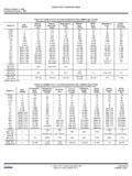
5 MAX. UnitDiode Forward Voltage VF IF = 10 mA V Reverse CurrentIR VR = 5 V 5 A Terminal Capacitance Ct V = 0 V, f = MHz 30 pF Transistor Collector to Emitter Dark Current ICEO VCE = 350 V, IF = 0 mA 400 nA Coupled Current Transfer Ratio (IC/IF) CTR IF = 1 mA, VCE = 2 V 1 500 4 000 6 500 % Collector Saturation Voltage VCE (sat) IF = 1 mA, IC = 2 mA V Isolation Resistance RI-O VI-O = kVDC1011 Isolation CapacitanceCI-OV = 0 V, f = MHz pF Rise Time*1tr VCC = 5 V, IC = 10 mA, RL = 100 100 s Fall Time *1tf100*1 Test circuit for switching time(PW = 1 ms, Duty cycle = 1/10)Pulse inputVCCVOUTRL = 100 50 IFData Sheet PN10233EJ03V0DS7PS2533-1,PS2533L-1 TYPICAL CHARACTERISTICS (TA = 25 C, unless otherwise specified) mW/ C150100500255075100125150 Ambient Temperature TA ( C)Diode Power Dissipation PD (mW)DIODE POWER DISSIPATION mW/ C4003002001000255075100125150 Ambient Temperature TA ( C)Transistor Power Dissipation PC (mW)TRANSISTOR POWER DISSIPATIONvs.
6 AMBIENT TEMPERATURE+25 C0 C 25 C 55 CTA = +100 C+75 C+50 Voltage VF (V)Forward Current IF (mA)FORWARD CURRENT VOLTAGEIF = mA16014012010080604020021345687 Collector to Emitter Voltage VCE (V)Collector Current IC (mA)COLLECTOR CURRENT TO EMITTER VOLTAGEVCE = 350 V 50 250255075100100 n10 n1 n100 p10 1 Ambient Temperature TA ( C)Collector to Emitter Dark Current ICEO (A)COLLECTOR TO EMITTER DARKCURRENT vs. AMBIENT TEMPERATUREIF= Saturation Voltage VCE (sat) (V)Collector Current IC (mA)COLLECTOR CURRENT SATURATION VOLTAGER emark The graphs indicate nominal characteristics. Data Sheet PN10233EJ03V0DS8 PS2533-1,PS2533L-1 LONG TERM CTR DEGRADATIONTime (Hr)CTR (Relative Value) = 1 mA,TA = 25 CIF = 1 mA,TA = 60 CFREQUENCY RESPONSE Frequency f (kHz)Normalized Gain Gv50 10 5 15 20 25 = 1 k 100 10 VCE = 4 V, Vin = Vp-pRLVinVout1 k 47 1 F Normalized to at TA = 25 C,IF = 1 mA, VCE = 2 50 252550751000 Ambient Temperature TA ( C)Normalized Current Transfer Ratio CTRNORMALIZED CURRENT TRANSFERRATIO vs.
7 AMBIENT TEMPERATUREVCE = 2 VSample AB5 0004 0003 0001 00002 Current IF (mA)Current Transfer Ratio CTR (%)CURRENT TRANSFER RATIO CURRENTVCC = 10 V, IC = 10 mAtrtdtstf500100501015201002005001 k2 k50 Load Resistance RL ( )Switching Time t ( s) SWITCHING TIME RESISTANCER emark The graphs indicate nominal characteristics. Data Sheet PN10233EJ03V0DS9PS2533-1,PS2533L-1 TAPING SPECIFICATIONS (Unit : mm) Tape DirectionPS2533L-1-F3 Outline and Dimensions (Tape) + 0 Outline and Dimensions (Reel)Packing: 2 000 330 to edge of <R>Data Sheet PN10233EJ03V0DS10 PS2533-1,PS2533L-1 NOTES ON HANDLING 1. Recommended soldering conditions(1) Infrared reflow soldering Peak reflow temperature260 C or below (package surface temperature) Time of peak reflow temperature10 seconds or less Time of temperature higher than 220 C60 seconds or less Time to preheat temperature from 120 to 180 C 120 30 s Number of reflowsThree FluxRosin flux containing small amount of chlorine (The flux with a maximum chlorine content of Wt% is recommended.)
8 120 30 s(preheating)220 C180 CPackage Surface Temperature T ( C)Time (s)Recommended Temperature Profile of Infrared Reflow(heating)to 10 sto 60 s260 C C(2) Wave soldering Temperature260 C or below (molten solder temperature) Time10 seconds or less Preheating conditions120 C or below (package surface temperature) Number of timesOne (Allowed to be dipped in solder including plastic mold portion.) FluxRosin flux containing small amount of chlorine (The flux with a maximum chlorine content of Wt% is recommended.) (3) Soldering by soldering iron Peak temperature (lead part temperature) 350 C or below Time (each pins)3 seconds or less FluxRosin flux containing small amount of chlorine (The flux with a maximum chlorine content of Wt% is recommended.) (a) Soldering of leads should be made at the point to mm from the root of the lead.(b) Please be sure that the temperature of the package would not be heated over 100 Sheet PN10233EJ03V0DS11PS2533-1,PS2533L-1(4) Cautions FluxesAvoid removing the residual flux with freon-based and chlorine-based cleaning Cautions regarding noiseBe aware that when voltage is applied suddenly between the PHOTOCOUPLER s input and output or betweencollector-emitters at startup, the output transistor may enter the on state, even if the voltage is within the absolutemaximum Measurement conditions of current transfer ratios (CTR), which differ according to photocouplerCheck the setting values before use, since the forward current conditions at CTR measurement differ accordingto using products other than at the specified forward current, the characteristics curves may differ from thestandard curves due to CTR value variations or the like.
9 Therefore, check the characteristics under the actualoperating conditions and thoroughly take variations or the like into consideration before CAUTIONS against static electricity when storage at a high temperature and high Sheet PN10233EJ03V0DS12 PS2533-1,PS2533L-1 SPECIFICATION OF VDE MARKS LICENSE DOCUMENT (VDE0884) ParameterSymbolSpeckUnitClimatic test class (IEC 60068-1/DIN EN 60068-1) 55/100/21 Dielectric strength maximum operating isolation voltage Test voltage (partial discharge test, procedure a for type test and random test)Upr = UIORM, Pd < 5 pC UIORM Upr 890 1 335 VpeakVpeak Test voltage (partial discharge test, procedure b for all devices test) Upr = UIORM, Pd < 5 pC Upr1 669 Vpeak Highest permissible overvoltage UTR8 000 Vpeak Degree of pollution (DIN EN 60664-1 VDE0110 Part 1) 2 Comparative tracking index (IEC 60112/DIN EN 60112 (VDE 0303 Part 11)) CTI 175 Material group (DIN EN 60664-1 VDE0110 Part 1) III a Storage temperature range Tstg 55 to +150 C Operating temperature range TA 55 to +100 CIsolation resistance, minimum value VIO = 500 V dc at TA = 25 C VIO = 500 V dc at TA MAX.
10 At least 100 C Ris MIN. Ris MIN. 10121011 Safety maximum ratings (maximum permissible in case of fault, see thermal derating curve) Package temperature Current (input current IF, Psi = 0) Power (output or total power dissipation) Isolation resistance VIO = 500 V dc at TA = 175 C (Tsi) Tsi Isi Psi Ris MIN. 175 400 700 109 CmAmW <R> PS2533-1,PS2533L-1 Caution GaAs Products This product uses gallium arsenide (GaAs). GaAs vapor and powder are hazardous to human health if inhaled or ingested, so please observe the following points. Follow related laws and ordinances when disposing of the product. If there are no applicable lawsand/or ordinances, dispose of the product as recommended Commission a disposal company able to (with a license to) collect, transport and dispose ofmaterials that contain arsenic and other such industrial waste Exclude the product from general industrial waste and household garbage, and ensure that theproduct is controlled (as industrial waste subject to special control) up until final disposal.