Transcription of PHOTODIODE CHARACTERISTICS
1 1 UDT Sensors Inc. Phone: 310-978-0516 Fax: 310-644-1727 http:\\ CHARACTERISTICSS ilicon photodiodes are semiconductor devices responsive to high-energy particles and photons. Photodiodes operate by absorption ofphotons or charged particles and generate a flow of current in an ex-ternal circuit, proportional to the incident power. Photodiodes can beused to detect the presence or absence of minute quantities of lightand can be calibrated for extremely accurate measurements from in-tensities below 1 pW/cm2 to intensities above 100 mW/cm2. Siliconphotodiodes are utilized in such diverse applications as spectroscopy,photography, analytical instrumentation, optical position sensors, beamalignment, surface characterization, laser range finders, optical com-munications, and medical imaging DIFFUSED SILICON PHOTODIODECONSTRUCTIONP lanar diffused silicon photodiodes are simply P-N junction diodes.
2 AP-N junction can be formed by diffusing either a P-type impurity (an-ode), such as Boron, into a N-type bulk silicon wafer, or a N-typeimpurity, such as Phosphorous, into a P-type bulk silicon wafer. Thediffused area defines the PHOTODIODE active area. To form an ohmiccontact another impurity diffusion into the backside of the wafer isnecessary. The impurity is an N-type for P-type active area and P-typefor an N-type active area. The contact pads are deposited on the frontactive area on defined areas, and on the backside, completely coveringthe device. The active area is then deposited on with an anti-reflectioncoating to reduce the reflection of the light for a specific predefinedwavelength.
3 The non-active area on the top is covered with a thicklayer of silicon oxide. By controlling the thickness of bulk substrate,the speed and responsivity of the PHOTODIODE can be controlled. Notethat the photodiodes, when biased, must be operated in the reversebias mode, a negative voltage applied to anode and positive volt-age to 1. Planar diffused silicon photodiodePRINCIPLE OF OPERATIONS ilicon is a semiconductor with a band gap energy of eV at roomtemperature. This is the gap between the valence band and the con-duction band. At absolute zero temperature the valence band is com-pletely filled and the conduction band is vacant.
4 As the temperatureincreases, the electrons become excited and escalate from the valenceband to the conduction band by thermal energy. The electrons canalso be escalated to the conduction band by particles or photons withenergies greater than , which corresponds to wavelengths shorterthan 1100 nm. The resulting electrons in the conduction band are freeto conduct to concentration gradient, the diffusion of electrons from the N-type region to the P-type region and the diffusion of holes from the P-type region to the N-type region, develops a built-in voltage acrossthe junction. The inter-diffusion of electrons and holes between the Nand P regions across the junction results in a region with no free carri-ers.
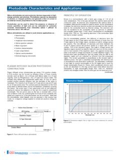
5 This is the depletion region. The built-in voltage across the deple-tion region results in an electric field with maximum at the junctionand no field outside of the depletion region. Any applied reverse biasadds to the built in voltage and results in a wider depletion electron-hole pairs generated by light are swept away by drift inthe depletion region and are collected by diffusion from the undepletedregion. The current generated is proportional to the incident light orradiation power. The light is absorbed exponentially with distance andis proportional to the absorption coefficient. The absorption coeffi-cient is very high for shorter wavelengths in the UV region and is smallfor longer wavelengths (Figure 2).
6 Hence, short wavelength photonssuch as UV, are absorbed in a thin top surface layer while silicon be-comes transparent to light wavelengths longer than 1200 nm. More-over, photons with energies smaller than the band gap are not absorbedat 2. Penetration depth of light into silicon substrate for various CHARACTERISTICSA silicon PHOTODIODE can be represented by a current source in parallelwith an ideal diode (Figure. 3). The current source represents thecurrent generated by the incident radiation, and the diode representsN-Type SubstrateP+N+Depletion RegionAR CoatingSiO2 Contact MetalActive Area DiameterAnode (+)Cathode (-)1E-051E-041E-031E-02 Penetration Depth (mm)350 4004505005506006507007508008509009501000 Wavelength (nm)2 UDT Sensors Inc.
7 Phone: 310-978-0516 Fax: 310-644-1727 http:\\ CHARACTERISTICSF igure 3. Equivalent Circuit for the silicon photodiodethe p-n junction. In addition, a junction capacitance (Cj) and a shuntresistance (RSH) are in parallel with the other components. Series re-sistance (RS) is connected in series with all components in this Resistance, RSHS hunt resistance is the slope of the current-voltage curve of the photo-diode at the origin, V=0. Although an ideal PHOTODIODE shouldhave a shunt resistance of infinite, actual values range from 10s to1000s of Mega ohms. Experimentally it is obtained by applying 10mV, measuring the current and calculating the resistance.
8 Shunt resis-tance is used to determine the noise current in the PHOTODIODE with nobias (photovoltaic mode). For best PHOTODIODE performance the high-est shunt resistance is Resistance, RSSeries resistance of a PHOTODIODE arises from the resistance of the con-tacts and the resistance of the undepleted silicon (Figure 1). It is givenby:()CdSSRAWWR+=( 1 )Where WS is the thickness of the substrate, Wd is the width of thedepleted region, A is the diffused area of the junction, is the resistiv-ity of the substrate and RC is the contact resistance. Series resistance isused to determine the linearity of the PHOTODIODE in photovoltaic mode(no bias, V=0).
9 Although an ideal PHOTODIODE should have no seriesresistance, typical values ranging from 10 to 1000 ohm is Capacitance, CJThe boundaries of the depletion region act as the plates of a parallelplate capacitor (Figure 1). The junction capacitance is directly pro-portional to the diffused area and inversely proportional to the widthof the depletion region. In addition, higher resistivity substrates havelower junction capacitance. Furthermore, the capacitance is depen-dent on the reverse bias as follows:()biASiSiJVVAC+=002( 2 )Figure 4. Capacitance of PIN-RD100 versus Reverse Bias Voltagewhere 0= F/cm, is the permittivity of free space, Si= the silicon dielectric constant, = 1400 cm2/Vs is the mobility of theelectrons at 300 K, is the resistivity of the silicon, Vbi is the built-involtage of silicon and VA is the applied bias.
10 Figure 4 shows the depen-dence of the capacitance on the applied reverse bias voltage. Junctioncapacitance is used to determine the speed of the response of the Time and Frequency Response, tr / tf / f3dBThe rise time and fall time of a PHOTODIODE is defined as the time forthe signal to rise or fall from 10% to 90% or 90% to 10% of the finalvalue respectively. This parameter can be also expressed as frequencyresponse, which is the frequency at which the PHOTODIODE output de-creases by 3dB. It is roughly approximated ( 3 )There are three factors defining the response time of a , the charge collection time of the carriers in the depletedregion of the , the charge collection time of the carriers in theundepleted region of the , the RC time constant of the diode-circuit is determined by tRC= RC, where R, is the sum of the diodeseries resistance and the load resistance (RS + RL), and C, is the sum ofthe PHOTODIODE junction and the stray capacitances (Cj+CS).