Transcription of PL-2303HX Edition (Chip Rev D) USB to Serial Bridge ...
1 PL-2303HX Edition (Chip Rev D) USB to Serial Bridge Controller Product Datasheet Document Revision: Document Release: April 16, 2007 Prolific Technology Inc. 7F, No. 48, Sec. 3, Nan Kang Rd. Nan Kang, Taipei 115, Taiwan, Telephone: +886-2-2654-6363 Fax: +886-2-2654-6161 E-mail: Revised Date: April 16, 2007 PL-2303HX (Rev D) Product Datasheet - 2 - Document Version Disclaimer All the information in this document is subject to change without prior notice. Prolific Technology Inc. does not make any representations or any warranties (implied or otherwise) regarding the accuracy and completeness of this document and shall in no event be liable for any loss of profit or any other commercial damage, including but not limited to special, incidental, consequential, or other damages. Trademarks The Prolific logo is a registered trademark of Prolific Technology Inc. All brand names and product names used in this document are trademarks or registered trademarks of their respective holders.
2 Copyrights Copyright 2007 Prolific Technology Inc., All rights reserved. No part of this document may be reproduced or transmitted in any form by any means without the express written permission of Prolific Technology Inc. Revised Date: April 16, 2007 PL-2303HX (Rev D) Product Datasheet - 3 - Document Version Revision History Revision Description Date Added Windows Vista and XP Logo Driver information Added USB-IF Logo TID information April 16, 2007 Sec. : Modified QFN diagram to add IC bottom PAD information June 30, 2006 PL-2303HX (Chip Rev D) Datasheet Formal Release November 23, 2005 Revised Date: April 16, 2007 PL-2303HX (Rev D) Product Datasheet - 4 - Document Version Table of Contents 8 FUNCTIONAL BLOCK 9 10 PIN ASSIGNMENT 11 SSOP28 11 QFN32 12 PIN ASSIGNMENT & 13 SSOP28 13 QFN32 14 USB STANDARD 15 Device 15 Configuration 15 interface 16 Endpoint 1 Descriptor: Interrupt Input 16 Endpoint 2 Descriptor: Bulk Data Output 16 Endpoint 3 Descriptor: Bulk Data Input 17 String 17 USB STANDARD 18 DATA FORMATS & PROGRAMMABLE BAUD RATE 19 DC & TEMPERATURE 20 Absolute Maximum 20 DC 20 Clock 21 Temperature 22 Leakage Current and 22 Power-On 22 OUTLINE 23 SSOP28 23 QFN32 24 Revised Date.
3 April 16, 2007 PL-2303HX (Rev D) Product Datasheet - 5 - Document Version REEL PACKING 25 Carrier Tape (SSOP-28).. 25 Reel 26 ORDERING 26 Revised Date: April 16, 2007 PL-2303HX (Rev D) Product Datasheet - 6 - Document Version List of Figures Figure 2-1 Block Diagram of PL-2303HX (Rev D).. 9 Figure 4-1 Pin Assignment Outline of PL-2303HX (Rev D) Figure 4-2 Pin Assignment Outline of PL-2303HX (Rev D) 12 Figure 10-1 Power-On Reset 22 Figure 10-1 Outline Diagram of PL-2303HX (Rev D) SSOP28 .. 23 Figure 10-2 Outline Diagram of PL-2303HX (Rev D) 24 Figure 11-1a SSOP28 Carrier 25 Figure 11-1b IC Reel 25 Figure 11-2 Reel Dimension .. 26 List of Tables Table 5-1 Pin Assignment & Description (SSOP28).. 13 Table 5-2 Pin Assignment & Description (QFN32).. 14 Table 6-1 Device Descriptor .. 15 Table 6-2 Configuration 15 Table 6-3 interface 16 Table 7-4 Endpoint1 16 Table 6-5 Endpoint2 16 Table 6-6 Endpoint3 17 Table 6-7a String Descriptor Language 17 Table 6-7b String Descriptor Manufacturer.
4 17 Table 6-7c String Descriptor 18 Table 6-7d String Descriptor Serial 18 Table 8-1 Supported Data Formats .. 19 Table 8-2 Baud Rate 19 Table 9-1 Absolute Maximum 20 Table 9-2a Operating Voltage and Suspend 20 Table 9-2b I/O 20 Table 9-2c Serial I/O Pins .. 21 Table 9-2d Serial I/O 21 Table 9-2e Serial I/O 21 Table 9-3 Clock 21 Table 9-4 Temperature 22 Table 9-5 Leakage Current and 22 Table 9-6 Power-On 22 Revised Date: April 16, 2007 PL-2303HX (Rev D) Product Datasheet - 7 - Document Version Table 10-1 Package Dimension .. 23 Table 11-2 Reel Part Number 26 Table 12-1 Ordering Information .. 26 Revised Date: April 16, 2007 PL-2303HX (Rev D) Product Datasheet - 8 - Document Version Features Fully Compliant with USB Specification (Full-Speed) On Chip USB transceiver , 5V regulator On-chip 96 MHz clock generator Supports RS-422/RS-485 like Serial interface (TXD, DTR_N, and RTS_N pins should be externally pulled-up to 5V) Supports RS232-like Serial interface o Full-duplex transmitter and receiver (TXD and RXD) o Six MODEM control pins (RTS, CTS, DTR, DSR, DCD, and RI)
5 O 5, 6, 7 or 8 data bits o Odd, Even, Mark, Space, or None parity mode o One, one and a half, or two stop bits o Parity error, frame error, and Serial break detection o Programmable baud rate from 75 bps to 12M bps o External RS232 driver power down control o Independent power source for Serial interface Extensive Flow Control Mechanism o Adjustable high/low watermark level o Automatic hardware flow control with CTS/RTS(1) or DSR/DTR(2) o Automatic software flow control with XON/XOFF o Inbound data buffer overflow detection Configurable 512-byte bi-directional data buffer o 256-byte outbound buffer and 256-byte inbound buffer; or o 128-byte outbound buffer and 384-byte inbound buffer Supports remote wake-up from MODEM input signals Four (4) General Purpose I/O (GP0, GP1, GP2, & GP3) pins & Four (4) Auxiliary General Purpose I/O (RI_N, DSR_N, DCD_N, & CTS_N) pins.
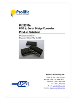
6 On-chip OTP (One Time Programming) ROM for startup device configurations Hardware backward compatible with PL-2303H Provides drivers support for Windows, Mac OS, Linux, and WinCE Windows XP Certified Logo Drivers (x86 driver only) Windows Vista Certified Logo Drivers (x86 and x64 drivers) USB-IF Logo Compliant with TID 40000100 Small footprint 28-pin SSOP or 32-pin QFN IC package Notes: (1) CTS/RTS Hardware Flow Control supports either low-level active or high-level active. (2) For DSR/DTR Hardware Flow Control support, please contact Prolific FAE for more information. Revised Date: April 16, 2007 Functional Block Diagram 96 MHz Clock GeneratorUSB to Digital LockLoopUSB to Serial interface EngineControl EndpointInterrupt EndpointBulk-inEndpointBulk-OutEndpoint2 56/384 ByteInbound DataBuffer256/128 ByteOutbound DataBufferRS232 / RS-422 / RS-485 LikeSerial interface Engine256-BytesOTP ROMH ardware ROMD efault DescriptorPL-2303 HXDRS-232/RS-422/RS-485 Like InterfaceUSB Host Figure 2-1 Block Diagram of PL-2303HX (Rev D) PL-2303HX (Rev D) Product Datasheet - 9 - Document Version Revised Date: April 16, 2007 PL-2303HX (Rev D) Product Datasheet - 10 - Document Version Introduction PL-2303HX provides a convenient solution for connecting an RS232-like full-duplex asynchronous Serial device to any Universal Serial Bus (USB) capable host.
7 PL-2303HX highly compatible drivers could simulate the traditional COM port on most operating systems allowing the existing applications based on COM port to easily migrate and be made USB ready. By taking advantage of USB bulk transfer mode, large data buffers, and automatic flow control, PL-2303HX is capable of achieving higher throughput compared to traditional UART (Universal Asynchronous Receiver Transmitter) ports. When real RS232 signaling is not required, baud rate higher than 115200 bps could be used for even higher performance. The flexible baud rate generator of PL-2303HX could be programmed to generate any rate between 75 bps to 12M bps. PL-2303HX is exclusively designed for mobile and embedded solutions in mind, providing a small footprint that could easily fit in to any connectors and handheld devices. With very small power consumption in either operating or suspend mode, PL-2303HX is perfect for bus powered operation with plenty of power left for the attached devices.
8 Flexible signal level requirement on the RS232-like Serial port side also allows PL-2303HX to connect directly to any ~ range devices. Revised Date: April 16, 2007 Pin Assignment Outline SSOP28 Package PL-2303HX (Rev D)1 TXD2 DTR_N3 RTS_N4 VDD_3255 RXD6RI_N7 GND8NC9 DSR_N10 DCD_N11 CTS_N12 SHTD_N13GP314GP228 RESERVED27NC26 TEST25 GND24NC23GP122GP021NC20 VDD_519 RESET_N18 GND17VO_3316DM15DP Figure 4-1 Pin Assignment Outline of PL-2303HX (Rev D) SSOP28 PL-2303HX (Rev D) Product Datasheet - 11 - Document Version Revised Date: April 16, 2007 QFN32 Package RTS_NNCGNDGNDTESTRESERVEDNCNCTXDDTR_NVDD _325 RXDRI_NGNDVDD_33 DSR_NDCD_NCTS_NSHTD_NGP3GP2 NCNCDPDMNCGP1GP0 NCVDD_5 RESET_NVO_33PL-2303 HXD1 Exp o sed Di e Pad co n n ects to VO _33 Figure 4-2 Pin Assignment Outline of PL-2303HX (Rev D) QFN32 Warning: The exposed center die pad of the PL-2303HX QFN package is connected (bonded) to the pin VO_33 so it is very important to design the PCB layout wherein this exposed die pad won t get grounded on the PCB when mounted.
9 PL-2303HX (Rev D) Product Datasheet - 12 - Document Version Revised Date: April 16, 2007 PL-2303HX (Rev D) Product Datasheet - 13 - Document Version Pin Assignment & Description Pin Type Abbreviation: I: Input O: Output B: Bidirectional I/O P: Power/Ground SSOP28 Package Table 5-1 Pin Assignment & Description (SSOP28) Pin # Name Type Description 1 TXD O (1) Serial Port (Transmitted Data) 2 DTR_N O (1) Serial Port (Data Terminal Ready) 3 RTS_N O (1) Serial Port (Request To Send) 4 VDD_325 P RS232 VDD. The power pin for the Serial port signals. When the Serial port is , this should be When the Serial port is , this should be The range can be from ~ 5 RXD I (2) Serial Port (Received Data) 6 RI_N B (2) Serial Port (Ring Indicator); or Auxiliary General Purpose I/O Port when enabled(7).
10 7 GND P Ground 8 NC - No Connection 9 DSR_N B (2) Serial Port (Data Set Ready); or Auxiliary General Purpose I/O Port when enabled(7). 10 DCD_N B (2) Serial Port (Data Carrier Detect); or Auxiliary General Purpose I/O Port when enabled(7). 11 CTS_N B (2) Serial Port (Clear to Send); or Auxiliary General Purpose I/O Port when enabled(7). 12 SHTD_N O (3)RS232 transceiver Shut Down Control 13 GP3 I/O Auxiliary GPIO Pin 3 (Default output high mode) (6)14 GP2 I/O Auxiliary GPIO Pin 2 (Default output high mode) (6)15 DP B USB Port D+ signal 16 DM B USB Port D- signal 17 VO_33 P Regulator Power Output, 18 GND P Ground 19 RESET_N I (4)External System Reset (Active Low) 20 VDD_5 P USB Port VBUS, 5V Power. ( for OTPROM writing voltage).