Transcription of Plasma Etching System and its Applications to 45 ... - Hitachi
1 Hitachi Review Vol. 56 (2007), No. 3 57. Plasma Etching System and its Applications to 45 32-nm leading -edge Devices Hiromichi Enami OVERVIEW: Maintaining the process accuracy of leading -edge Masamichi Sakaguchi semiconductor devices has recently become quite difficult. Dry Etching , in particular, is facing many new challenges, such as the application of Naoshi Itabashi immersion lithography photo resists, dual metal materials, low-k and high- Masaru Izawa k materials, in addition to the basic requirements of cost and performance. Hitachi has developed excellent dry- Etching equipment and application processes for manufacturing complicated devices that are based on a simplified chamber structure.
2 These processes achieved the targets of 45 . 32-nm nodes while simultaneously accomplishing high throughput, high yield, and high productivity. A critical dimension uniformity of nm, a line width roughness of nm, and an isolation-dense bias of nm have been achieved for gate Etching . Etching rates of 300 nm/min, critical dimension shifts of < nm, and critical dimension uniformity of 3 nm have been attained for multilayer masks. Time-dependent changes could be reduced to using process-control technology. Hitachi has already confirmed these features in 45-nm-node pre-manufacturing. INTRODUCTION a 300-mm wafer may have a large impact on final 45-nm-NODE semiconductor devices are being yields.
3 This situation is conspicuous in 65-nm nodes produced worldwide and 32-nm-node processes are or less and thus strict targets for uniformity are being developed. Hitachi has developed excellent dry- required by the end users of equipment. Etching equipment and processes that can achieve high Improvements to productivity on the other hand, that throughput, high yield, and high productivity in the have driven down wafer costs are also serious issues. manufacture of these complex devices. Fig. 1 outlines tactics used for increasing productivity. Dry Etching is a chemical reaction between Equipment productivity clearly plays a major role in semiconductor-wafer surface materials and reactive decreasing costs.
4 However, the major index, OEE. gases within the Plasma . Photo-resist materials create patterns on semiconductor wafers during the lithography process and serve to protect areas where Present reactions are not required. The lithography process Feature size Logarithmic $ per function actually creates feature sizes (patterns) that are smaller 12 14%. than the exposure wavelength (193 nm for ArF excimer Wafer size exposure) used to create these patterns for leading - Yield improvement edge semiconductor devices. Therefore, many Other productivity Equipment technologies to enhance resolution have been widely equipment productivity applied that often have an adverse impact on dry 25 30% (per year).
5 Etching . Dry- Etching technologies must not only improvements Historic curve overcome the negative impact on enhancing resolution, Time but also improve patterning accuracy. New concerns regarding yield-related issues are Fig. 1 Tactics for Improving Productivity. already being seen in addition to typical concerns The chip functional cost should be reduced by 25 to 30% per regarding manufacturing variations in 45 32-nm year by reducing feature size, improving yield, and increasing nodes. The reason is that even very small variations productivity. The measures for improving productivity are the from the CD (critical dimension) or taper angle within most important.
6 Plasma Etching System and its Applications to 45 32-nm leading -edge Devices 58. (overall equipment effectiveness), of equipment productivity is still lower than 50%. The main reasons Equipment settings RF power, pressure Disturbing factors for low OEE are QC (quality control) operations using the NPW (non-product wafer), scheduled down Treatment environment Environment sensor time, and unscheduled down time. As these are Electron density and Plasma impedance distribution Plasma emission common conditions throughout the world, the ITRS Ion density & distribution Mass analyzer (International Technology Roadmap for Semiconductors) Surface voltage & distribution Electron & ion temperature is discussing methods of increasing OEE.
7 ITRS listed six major items (1),(2) Wafer state Wafer state sensor Etching speed selectivity (1) Resource-consumption management RF: radio frequency (2) Time-dependent performance changes and Fig. 2 Relationship Between Equipment Settings and Wafer compensation State. (3) Machine-to-machine differences and adjustments Wafer states are not directly related to equipment settings in the (4) NPW management and control process equipment. There are treatment environments between (5) Chamber wet cleaning and specifications the equipment settings and wafer states, and they are (6) Equipment maintenance and rules susceptible to many disturbing factors.
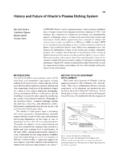
8 These issues are being studied globally and almost all solutions have now been standardized. Hitachi , as an equipment vendor of a critical process tools, is designing technologies that will conform to ITRS. requirements, , it is applying stabilizing measures to decrease machine-to-machine variation and time- dependent changes. The details are described below. New gates DESIGN OF Hitachi EQUIPMENT Gas distribution and SIMPLIFIED Etching REACTIONS byproduct control The relationship between process settings and process results is plotted in Fig. 2. Process results are Fig. 3 Completely Symmetrical Chamber Structure. not generally directly controlled by process settings A completely symmetrical layout for all functional parts achieved a simple distribution for efficient Etching .
9 Etch uniformity can because the wafer itself is exposed in a reaction easily be modified by adjusting a few tuning knobs. environment that is subjected to many disturbing factors. These influences are much more serious in leading -edge manufacturing. Therefore, measures for accomplished by applying coaxially installed turbo stabilization cannot be introduced without reducing molecular pumps, symmetrically designed electrodes, the influence of disturbing factors. and specially designed variable conductance valves Several countermeasures have been investigated to to a completely symmetrical reaction chamber, as reduce the complexity of present Etching process.
10 We shown in Fig. 3. Etching can be improved to have the need to: required symmetrical distribution using this design. (1) Establish a simple Etching model through High-volume exhaust systems and low-pressure improving hardware, reactions, which are possible using a high-frequency (2) Set up independent tuning knobs to adjust Etching discharge mechanism with electromagnetic coils, will and install sensors to monitor this,(5) be used to reduce the influence of disturbing factors (3) Position the knobs and optimize the process based in the next step. on the simplified Etching model, and Appropriate tuning knobs with features below were (4) Construct AEC (advanced equipment control)/APC introduced to this new concept for dry- Etching (advanced process control) systems based on the equipment.