Transcription of PMDT290UCE 20 / 20 V, 800 / 550 mA N/P-channel Trench …
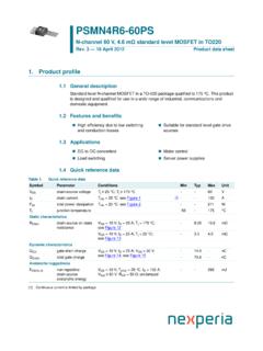
1 PMDT290 UCE. 20 / 20 V, 800 / 550 mA N/P-channel Trench MOSFET. Rev. 1 6 October 2011 Product data sheet 1. Product profile General description Complementary N/P-channel enhancement mode Field-Effect Transistor (FET) in an ultra small and flat lead SOT666 Surface-Mounted Device (SMD) plastic package using Trench MOSFET technology. Features and benefits Very fast switching ESD protection up to 2 kV. Trench MOSFET technology AEC-Q101 qualified Applications Relay driver Low-side loadswitch High-speed line driver Switching circuits Quick reference data Table 1. Quick reference data Symbol Parameter Conditions Min Typ Max Unit TR1 (N-channel), Static characteristics RDSon drain-source on-state VGS = V; ID = 500 mA; Tj = 25 C - 290 380 m . resistance TR2 (P-channel), Static characteristics RDSon drain-source on-state VGS = V; ID = -400 mA; Tj = 25 C.
2 Resistance TR1 (N-channel). VDS drain-source voltage Tj = 25 C - - 20 V. VGS gate-source voltage -8 - 8 V. ID drain current VGS = V; Tamb = 25 C [1] - - 800 mA. TR2 (P-channel). VDS drain-source voltage Tj = 25 C - - -20 V. VGS gate-source voltage -8 - 8 V. ID drain current VGS = V; Tamb = 25 C [1] - - -550 mA. [1] Device mounted on an FR4 PCB, single-sided copper, tin-plated and mounting pad for drain 1 cm2. Nexperia PMDT290 UCE. 20 / 20 V, 800 / 550 mA N/P-channel Trench MOSFET. 2. Pinning information Table 2. Pinning information Pin Symbol Description Simplified outline Graphic symbol 1 S1 source TR1. 6 5 4 D1 D2. 2 G1 gate TR1. 3 D2 drain TR2. 4 S2 source TR2 G1 G2. 5 G2 gate TR2. 1 2 3. 6 D1 drain TR1. SOT666. S1 S2. 017aaa262. 3. Ordering information Table 3. Ordering information Type number Package Name Description Version PMDT290 UCE - plastic surface-mounted package; 6 leads SOT666.
3 4. Marking Table 4. Marking codes Type number Marking code PMDT290 UCE AF. 5. Limiting values Table 5. Limiting values In accordance with the Absolute Maximum Rating System (IEC 60134). Symbol Parameter Conditions Min Max Unit TR1 (N-channel). VDS drain-source voltage Tj = 25 C - 20 V. VGS gate-source voltage -8 8 V. ID drain current VGS = V; Tamb = 25 C [1] - 800 mA. VGS = V; Tamb = 100 C [1] - 500 mA. IDM peak drain current Tamb = 25 C; single pulse; tp 10 s - A. Ptot total power dissipation Tamb = 25 C [2] - 330 mW. [1] - 390 mW. Tsp = 25 C - 1090 mW. TR1 (N-channel), Source-drain diode IS source current Tamb = 25 C [1] - 370 mA. TR1 N-channel), ESD maximum rating VESD electrostatic discharge voltage HBM [3] - 2000 V. PMDT290 UCE All information provided in this document is subject to legal disclaimers. Nexperia 2017. All rights reserved Product data sheet Rev.
4 1 6 October 2011 2 of 20. Nexperia PMDT290 UCE. 20 / 20 V, 800 / 550 mA N/P-channel Trench MOSFET. Table 5. Limiting values continued In accordance with the Absolute Maximum Rating System (IEC 60134). Symbol Parameter Conditions Min Max Unit TR2 (P-channel). VDS drain-source voltage Tj = 25 C - -20 V. VGS gate-source voltage -8 8 V. ID drain current VGS = V; Tamb = 25 C [1] - -550 mA. VGS = V; Tamb = 100 C [1] - -350 mA. IDM peak drain current Tamb = 25 C; single pulse; tp 10 s - A. Ptot total power dissipation Tamb = 25 C [2] - 330 mW. [1] - 390 mW. Tsp = 25 C - 1090 mW. TR2 (P-channel), Source-drain diode IS source current Tamb = 25 C [1] - -370 mA. TR2 (P-channel), ESD maximum rating VESD electrostatic discharge voltage HBM [3] - 2000 V. Per device Ptot total power dissipation Tamb = 25 C [2] - 500 mW. Tj junction temperature -55 150 C.
5 Tamb ambient temperature -55 150 C. Tstg storage temperature -65 150 C. [1] Device mounted on an FR4 PCB, single-sided copper, tin-plated and mounting pad for drain 1 cm2. [2] Device mounted on an FR4 Printed-Circuit Board (PCB), single-sided copper; tin-plated and standard footprint. [3] Measured between all pins. 017aaa123 017aaa124. 120 120. Pder Ider (%) (%). 80 80. 40 40. 0 0. 75 25 25 75 125 175 75 25 25 75 125 175. Tj ( C) Tj ( C). Fig 1. Normalized total power dissipation as a Fig 2. Normalized continuous drain current as a function of junction temperature function of junction temperature PMDT290 UCE All information provided in this document is subject to legal disclaimers. Nexperia 2017. All rights reserved Product data sheet Rev. 1 6 October 2011 3 of 20. Nexperia PMDT290 UCE. 20 / 20 V, 800 / 550 mA N/P-channel Trench MOSFET.
6 017aaa361. 10. ID. (A) Limit RDSon = VDS/ID. 1. (1). (2). 10 1. (3). (4). (5). 10 2. 10 1 1 10 102. VDS (V). IDM = single pulse (1) tp = 1 ms (2) tp = 10 ms (3) DC; Tsp = 25 C. (4) tp = 100 ms (5) DC; Tamb = 25 C; drain mounting pad 1 cm2. Fig 3. Safe operating area TR1 (N-channel); junction to ambient; continuous and peak drain currents as a function of drain-source voltage 017aaa373. 10. ID. (A). Limit RDSon = VDS/ID. 1. (1). 10 1 (2). (3). (4). (5). 10 2. 10 1 1 10 102. VDS (V). IDM = single pulse (1) tp = 1 ms (2) tp = 10 ms (3) DC; Tsp = 25 C. (4) tp = 100 ms (5) DC; Tamb = 25 C; drain mounting pad 1 cm2. Fig 4. Safe operating area TR2 (P-channel); junction to ambient; continuous and peak drain currents as a function of drain-source voltage PMDT290 UCE All information provided in this document is subject to legal disclaimers.
7 Nexperia 2017. All rights reserved Product data sheet Rev. 1 6 October 2011 4 of 20. Nexperia PMDT290 UCE. 20 / 20 V, 800 / 550 mA N/P-channel Trench MOSFET. 6. Thermal characteristics Table 6. Thermal characteristics Symbol Parameter Conditions Min Typ Max Unit TR1 (N-channel). Rth(j-a) thermal resistance in free air [1] - 330 380 K/W. from junction to [2] - 280 320 K/W. ambient Rth(j-sp) thermal resistance - - 115 K/W. from junction to solder point TR2 (P-channel). Rth(j-a) thermal resistance in free air [1] - 330 380 K/W. from junction to [2] - 280 320 K/W. ambient Rth(j-sp) thermal resistance - - 115 K/W. from junction to solder point Per device Rth(j-a) thermal resistance in free air [1] - - 250 K/W. from junction to ambient [1] Device mounted on an FR4 Printed-Circuit Board (PCB), single-sided copper; tin-plated and standard footprint.
8 [2] Device mounted on an FR4 PCB, single-sided copper, tin-plated and mounting pad for drain 1 cm2. 017aaa064. 103. Zth(j-a) duty cycle = 1. (K/W) 102 0 10 1. 10 3 10 2 10 1 1 10 102 103. tp (s). FR4 PCB, standard footprint Fig 5. TR1: Transient thermal impedance from junction to ambient as a function of pulse duration; typical values PMDT290 UCE All information provided in this document is subject to legal disclaimers. Nexperia 2017. All rights reserved Product data sheet Rev. 1 6 October 2011 5 of 20. Nexperia PMDT290 UCE. 20 / 20 V, 800 / 550 mA N/P-channel Trench MOSFET. 017aaa065. 103. Zth(j-a) duty cycle = 1. (K/W). 102 0 10 1. 10 3 10 2 10 1 1 10 102 103. tp (s). FR4 PCB, mounting pad for drain 1 cm2. Fig 6. TR1: Transient thermal impedance from junction to ambient as a function of pulse duration; typical values 017aaa064.
9 103. Zth(j-a) duty cycle = 1. (K/W) 102 0 10 1. 10 3 10 2 10 1 1 10 102 103. tp (s). FR4 PCB, standard footprint Fig 7. TR2: Transient thermal impedance from junction to ambient as a function of pulse duration; typical values PMDT290 UCE All information provided in this document is subject to legal disclaimers. Nexperia 2017. All rights reserved Product data sheet Rev. 1 6 October 2011 6 of 20. Nexperia PMDT290 UCE. 20 / 20 V, 800 / 550 mA N/P-channel Trench MOSFET. 017aaa065. 103. Zth(j-a) duty cycle = 1. (K/W). 102 0 10 1. 10 3 10 2 10 1 1 10 102 103. tp (s). FR4 PCB, mounting pad for drain 1 cm2. Fig 8. TR2: Transient thermal impedance from junction to ambient as a function of pulse duration; typical values 7. Characteristics Table 7. Characteristics Symbol Parameter Conditions Min Typ Max Unit TR1 (N-channel), Static characteristics V(BR)DSS drain-source ID = 250 A; VGS = 0 V; Tj = 25 C 20 - - V.
10 Breakdown voltage VGSth gate-source threshold ID = 250 A; VDS = VGS; Tj = 25 C V. voltage IDSS drain leakage current VDS = 20 V; VGS = 0 V; Tj = 25 C - - 1 A. VDS = 20 V; VGS = 0 V; Tj = 150 C - - 10 A. IGSS gate leakage current VGS = 8 V; VDS = 0 V; Tj = 25 C - - 2 A. VGS = -8 V; VDS = 0 V; Tj = 25 C - - 2 A. VGS = V; VDS = 0 V; Tj = 25 C - - 500 nA. VGS = V; VDS = 0 V; Tj = 25 C - - 500 nA. RDSon drain-source on-state VGS = V; ID = 500 mA; Tj = 25 C - 290 380 m . resistance VGS = V; ID = 500 mA; Tj = 150 C - 460 610 m . VGS = V; ID = 200 mA; Tj = 25 C - 420 620 m . VGS = V; ID = 10 mA; Tj = 25 C - . gfs transfer conductance VDS = 10 V; ID = 200 mA; Tj = 25 C - - S. TR1 (N-channel), Dynamic characteristics QG(tot) total gate charge VDS = 10 V; ID = 500 mA; VGS = V; - nC. QGS gate-source charge Tj = 25 C - - nC. QGD gate-drain charge - - nC.