Transcription of Precision, High Speed, BiFET Quad Op Amp AD713
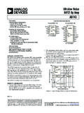
1 precision , high speed , BiFET quad Op Amp AD713 Rev. F Information furnished by analog devices is believed to be accurate and reliable. However, no responsibility is assumed by analog devices for its use, nor for any infringements of patents or other rights of third parties that may result from its use. Specifications subject to change without notice. No license is granted by implication or otherwise under any patent or patent rights of analog devices . Trademarks and registered trademarks are the property of their respective owners. One Technology Way, Box 9106, Norwood, MA 02062-9106, : Fax: 2002 2011 analog devices , Inc. All rights reserved. FEATURES AC performance 1 s settling to for 10 V step 20 V/ s slew rate total harmonic distortion (THD) 4 MHz unity gain bandwidth DC performance mV maximum offset voltage 8 V/ C typical drift 150 V/mV minimum open-loop gain 2 V p-p typical noise, Hz to 10 Hz True 14-bit accuracy Single version: AD711, dual version: AD712 Available in 16-lead SOIC, 14-lead PDIP and CERDIP APPLICATIONS Active filters quad output buffers for 12- and 14-bit DACs Input buffers for precision ADCs Photo diode preamplifier applications CONNECTION DIAGRAMS 00824-001AD713 TOP VIEW(Not to Scale)1234 OUTPUT14 IN13+IN12 VS115+IN106 IN97 OUTPUTOUTPUT IN+IN+VS+IN INOUTPUT84132 Figure 1.
2 14-Lead PDIP (N) and CERDIP (Q) Packages 00824-002NC = NO CONNECT. DO NOTCONNECT TO THIS IN2+IN3+VS4 OUTPUT16 IN15+IN14 VS13+IN5+IN12 IN6 IN11 OUTPUT7 OUTPUT10NC8NC94132AD713 TOP VIEW(Not to Scale) Figure 2. 16-Lead SOIC_W (RW) Package GENERAL DESCRIPTION The AD713 is a quad operational amplifier, consisting of four AD711 BiFET op amps. These precision monolithic op amps offer excellent dc characteristics plus rapid settling times, high slew rates, and ample bandwidths. In addition, the AD713 provides the close matching ac and dc characteristics inherent to amplifiers sharing the same monolithic die. The single-pole response of the AD713 provides fast settling: l s to This feature, combined with its high dc precision , makes the AD713 suitable for use as a buffer amplifier for 12- or 14-bit DACs and ADCs.
3 It is also an excellent choice for use in active filters in 12-, 14- and 16-bit data acquisition systems. Furthermore, the AD713 low total harmonic distortion (THD) level of and very close matching ac characteristics make it an ideal amplifier for many demanding audio applications. The AD713 is internally compensated for stable operation at unity gain. The AD713J is rated over the commercial temperature range of 0 C to 70 C. The AD713A is rated over the industrial temperature of 40 C to +85 C. The AD713 is offered in 16-lead SOIC, 14-lead PDIP, and 14-lead CERDIP packages. PRODUCT HIGHLIGHTS 1. The AD713 is a high speed BiFET op amp that offers excellent performance at competitive prices. It upgrades the performance of circuits using op amps such as the TL074, TL084, LT1058, LF347, and OPA404.
4 2. Slew rate is 100% tested for a guaranteed minimum of 16 V/ s (J and A grades). 3. The combination of analog devices , Inc., advanced processing technology, laser wafer drift trimming, and well-matched ion-implanted JFETs provides outstanding dc precision . Input offset voltage, input bias current and input offset current are specified in the warmed-up condition and are 100% tested. 4. Very close matching of ac characteristics between the four amplifiers makes the AD713 ideal for high quality active filter applications. AD713 Rev. F | Page 2 of 20 TABLE OF CONTENTS Features .. 1 1 Connection Diagrams .. 1 General Description .. 1 Product Highlights .. 1 Revision History .. 2 3 Absolute Maximum 5 Thermal Resistance .. 5 ESD 5 Typical Performance Characteristics.
5 6 Test Circuits .. 10 Theory of Operation .. 11 Measuring AD713 Settling Time .. 11 Power Supply Bypassing .. 11 A high speed Instrumentation Amplifier 12 A high speed 4-Op-Amp Cascaded Amplifier Circuit .. 12 high speed Op Amp Applications and Techniques .. 12 CMOS DAC Applications .. 14 Filter Applications .. 14 GIC and FDNR Filter Applications .. 15 Outline Dimensions .. 17 Ordering Guide .. 18 REVISION HISTORY 7/11 Rev. E to Rev. F Changes to Figure 2 .. 1 6/11 Rev. D to Rev. E Changed 8 V/ C Maximum Drift to 8 V/ C Typical Drift in Features Section .. 1 5/11 Rev. C to Rev. D Updated Format ..Universal Changes to Features Section, General Description Section, and Product Highlights Section .. 1 Deleted S, K, B, and T Grades 1 Changes to Table 3 Changes to Table 5 Added Typical Performance Characteristics Summary.
6 6 Change to Figure 7 .. 7 Changes to Figure 15, Figure 17, and Figure 18 .. 8 Deleted Figure 9 and Figure 10; Renumbered Sequentially ..9 Changes to Figure 23 Caption and Figure 24 Caption .. 10 Added Test Circuits 11 Moved Figures 26, Figure 27, and Figure 28 .. 11 Changes to Figure 12 Changes to DAC Buffers (I-to-V Converters) 13 Changes to Figure 37 and Table 14 Changed C1 to 14 Changes to Figure 43 and Figure 15 Updated Outline Dimensions .. 18 Changes to Ordering Guide .. 19 10/01 Rev. B to Rev. C Edits to Edits to Product Description ..1 Edits to Ordering Guide ..3 Edits to Metallization Photograph ..3 AD713 Rev. F | Page 3 of 20 SPECIFICATIONS VS = 15 V at TA = 25 C, unless otherwise noted. Table 1. AD713J/AD713A Parameter Test Conditions/Comments Min Typ Max Unit INPUT OFFSET VOLTAGE1 Initial Offset mV Offset
7 TMIN to TMAX 2 mV vs. Temp 5 V/ C vs. Supply 78 95 dB TMIN to TMAX 76 95 dB Long-Term Stability 15 V/Month INPUT BIAS CURRENT2 VCM = 0 V 40 150 pA VCM = 0 V at TMAX nA VCM = 10 V 55 200 pA INPUT OFFSET CURRENT VCM = 0 V 10 75 pA VCM = 0 V at TMAX
8 PA MATCHING CHARACTERISTICS Input Offset Voltage mV TMIN to TMAX mV Input Offset Voltage Drift 8 V/ C Input Bias Current 10 100 pA Crosstalk f = 1 kHz 130 dB f = 100 kHz 95 dB FREQUENCY RESPONSE Small Signal Bandwidth G = 1 MHz Full Power Response VO = 20 V p-p 200 kHz Slew Rate G = 1 16 20 V/ s Settling Time to s Total Harmonic Distortion f = 1 kHz; RL 2 k ; VO = 3 V rms % INPUT IMPEDANCE Differential3 3 1012|| ||pF Common Mode4 3 1012|| ||pF INPUT VOLTAGE RANGE Differential 20 V Common-Mode Voltage + V TMIN to TMAX 11 +13 V Common
9 Mode VCM = 10 V 78 88 dB Rejection Ratio TMIN to TMAX 76 84 dB VCM = 11 V 72 84 dB TMIN to TMAX 70 80 dB INPUT VOLTAGE NOISE Hz to 10 Hz 2 V p-p f = 10 Hz 45 nV/ Hz f = 100 Hz 22 nV/ Hz f = 1 kHz 18 nV/ Hz f = 10 kHz 16 nV/ Hz INPUT CURRENT NOISE f = 1 kHz pA/ Hz OPEN-LOOP GAIN VO = 10 V; RL 2 k 150 400 V/mV TMIN to TMAX 100 V/mV AD713 Rev.
10 F | Page 4 of 20 AD713J/AD713A Parameter Test Conditions/Comments Min Typ Max Unit OUTPUT CHARACTERISTICS Voltage RL 2 k +13/ + V TMIN to TMAX 12 + V Current Short circuit 25 mA POWER SUPPLY Rated Performance 15 V Operating Range 18 V Quiescent Current
