Transcription of Precision Instrumentation Amplifier AD524 - Datasheet Archive
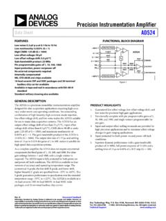
1 Precision Instrumentation Amplifier AD524 . FEATURES FUNCTIONAL BLOCK DIAGRAM. Low noise: V p-p at Hz to 10 Hz Low nonlinearity: (G = 1) INPUT 1 PROTECTION. High CMRR: 120 dB (G = 1000) AD524 . G = 10 13. Low offset voltage: 50 V 404 . G = 100 12. Low offset voltage drift: V/ C Vb 20k . 40 SENSE. Gain bandwidth product: 25 MHz G = 1000 11. 20k 20k . Pin programmable gains of 1, 10, 100, 1000 RG1 16. OUTPUT. Input protection, power-on/power-off RG2 3. 20k 20k . No external components required 20k . REFERENCE. Internally compensated 00500-001. + INPUT 2 PROTECTION. MIL-STD-883B and chips available 16-lead ceramic DIP and SOIC packages and 20-terminal Figure 1. leadless chip carrier available Available in tape and reel in accordance with EIA-481A. standard Standard military drawing also available GENERAL DESCRIPTION.
2 The AD524 is a Precision monolithic Instrumentation Amplifier higher linearity C grade are specified from 25 C to +85 C. designed for data acquisition applications requiring high accu- The S grade guarantees performance to specification over the racy under worst-case operating conditions. An outstanding extended temperature range 55 C to +125 C. The AD524 is combination of high linearity, high common-mode rejection, available in a 16-lead ceramic DIP, 16-lead SBDIP, 16-lead SOIC. low offset voltage drift, and low noise makes the AD524 suitable wide packages, and 20-terminal leadless chip carrier. for use in many data acquisition systems. PRODUCT HIGHLIGHTS. The AD524 has an output offset voltage drift of less than 1. The AD524 has guaranteed low offset voltage, offset 25 V/ C, input offset voltage drift of less than V/ C, CMR voltage drift, and low noise for Precision high gain above 90 dB at unity gain (120 dB at G = 1000), and maximum applications.
3 Nonlinearity of at G = 1. In addition to the outstanding dc specifications, the AD524 also has a 25 kHz bandwidth 2. The AD524 is functionally complete with pin program- (G = 1000). To make it suitable for high speed data acquisition mable gains of 1, 10, 100, and 1000, and single resistor systems, the AD524 has an output slew rate of 5 V/ s and settles programmable for any gain. in 15 s to for gains of 1 to 100. 3. Input and output offset nulling terminals are provided for As a complete Amplifier , the AD524 does not require any exter- very high Precision applications and to minimize offset nal components for fixed gains of 1, 10, 100 and 1000. For other voltage changes in gain ranging applications. gain settings between 1 and 1000, only a single resistor is required. 4. The AD524 is input protected for both power-on and The AD524 input is fully protected for both power-on and power-off fault conditions.
4 Power-off fault conditions. 5. The AD524 offers superior dynamic performance with a The AD524 IC Instrumentation Amplifier is available in four gain bandwidth product of 25 MHz, full power response of different versions of accuracy and operating temperature range. 75 kHz and a settling time of 15 s to of a 20 V step The economical A grade, the low drift B grade, and lower drift, (G = 100). Rev. F. Information furnished by Analog Devices is believed to be accurate and reliable. However, no responsibility is assumed by Analog Devices for its use, nor for any infringements of patents or other rights of third parties that may result from its use. Specifications subject to change without notice. No license is granted by implication or otherwise under any patent or patent rights of Analog Devices.
5 Trademarks and registered trademarks are the property of their respective owners. AD524 . SPECIFICATIONS. @ VS = 15 V, RL = 2 k and TA = +25 C, unless otherwise noted. All min and max specifications are guaranteed. Specifications shown in boldface are tested on all production units at the final electrical test. Results from those tests are used to calculate outgoing quality levels. Table 1. AD524A AD524B. Parameter Min Typ Max Min Typ Max Unit GAIN. Gain Equation (External Resistor Gain Programming). 40 ,000 40 ,000 . + 1 20% + 1 20%. RG RG . Gain Range (Pin Programmable) 1 to 1000 1 to 1000. Gain Error 1. G=1 %. G = 10 %. G = 100 %. G = 1000 %. Nonlinearity G=1 %. G = 10, G = 100 %. G = 1000 %. Gain vs. Temperature G=1 5 5 ppm/ C. G = 10 15 10 ppm/ C. G = 100 35 25 ppm/ C. G = 1000 100 50 ppm/ C.
6 VOLTAGE OFFSET (May be Nulled). Input Offset Voltage 250 100 V. vs. Temperature 2 V/ C. Output Offset Voltage 5 3 mV. vs. Temperature 100 50 V. Offset Referred to the Input vs. Supply G=1 70 75 dB. G = 10 85 95 dB. G = 100 95 105 dB. G = 1000 100 110 dB. INPUT CURRENT. Input Bias Current 50 25 nA. vs. Temperature 100 100 pA/ C. Input Offset Current 35 15 nA. vs. Temperature 100 100 pA/ C. Rev. F | Page 3 of 28. AD524 . AD524A AD524B. Parameter Min Typ Max Min Typ Max Unit INPUT. Input Impedance Differential Resistance 109 109 . Differential Capacitance 10 10 pF. Common-Mode Resistance 109 109 . Common-Mode Capacitance 10 10 pF. Input Voltage Range Maximum Differential Input Linear (VDL) 2 10 10 V. Maximum Common-Mode Linear (VCM)2 G G V. 12 V VD 12 V VD . 2 2 . Common-Mode Rejection DC to 60 Hz with 1 k Source Imbalance V.
7 G=1 70 75 dB. G = 10 90 95 dB. G = 100 100 105 dB. G = 1000 110 115 dB. OUTPUT RATING. VOUT, RL = 2 k 10 10 V. DYNAMIC RESPONSE. Small Signal 3 dB. G=1 1 1 MHz G = 10 400 400 kHz G = 100 150 150 kHz G = 1000 25 25 kHz Slew Rate V/ s Settling Time to , 20 V Step G = 1 to 100 15 15 s G = 1000 75 75 s NOISE. Voltage Noise, 1 kHz RTI 7 7 nV/ Hz RTO 90 90 nV Hz RTI, Hz to 10 Hz G=1 15 15 V p-p G = 10 2 2 V p-p G = 100, 1000 V p-p Current Noise Hz to 10 Hz 60 60 pA p-p SENSE INPUT. RIN 20 20 k 20%. IIN 15 15 A. Voltage Range 10 10 V. Gain to Output 1 1 %. REFERENCE INPUT. RIN 40 40 k 20%. IIN 15 15 A. Voltage Range 10 10 V. Gain to Output 1 1 %. Rev. F | Page 4 of 28. AD524 . AD524A AD524B. Parameter Min Typ Max Min Typ Max Unit TEMPERATURE RANGE. Specified Performance 25 +85 25 +85 C. Storage 65 +150 65 +150 C.
8 POWER SUPPLY. Power Supply Range 6 15 18 6 15 18 V. Quiescent Current mA. 1. Does not include effects of external resistor, RG. 2. VOL is the maximum differential input voltage at G = 1 for specified nonlinearity. VDL at the maximum = 10 V/G. VD = actual differential input voltage. Example: G = 10, VD = VCM = 12 V (10/2 V) = V. @ VS = 15 V, RL = 2 k and TA = +25 C, unless otherwise noted. All min and max specifications are guaranteed. Specifications shown in boldface are tested on all production units at the final electrical test. Results from those tests are used to calculate outgoing quality levels. Table 2. AD524C AD524S. Parameter Min Typ Max Min Typ Max Unit GAIN. Gain Equation (External Resistor Gain Programming). 40 ,000 40 ,000 . + 1 20% + 1 20%. RG RG . Gain Range (Pin Programmable) 1 to 1000 1 to 1000.
9 Gain Error 1. G=1 %. G = 10 %. G = 100 %. G = 1000 %. Nonlinearity G=1 %. G = 10, G = 100 %. G = 1000 %. Gain vs. Temperature G=1 5 5 ppm/ C. G = 10 10 10 ppm/ C. G = 100 25 25 ppm/ C. G = 1000 50 50 ppm/ C. VOLTAGE OFFSET (May be Nulled). Input Offset Voltage 50 100 V. vs. Temperature V/ C. Output Offset Voltage mV. vs. Temperature 25 50 V. Offset Referred to the Input vs. Supply G=1 80 75 dB. G = 10 100 95 dB. G = 100 110 105 dB. G = 1000 115 110 dB. Rev. F | Page 5 of 28. AD524 . AD524C AD524S. Parameter Min Typ Max Min Typ Max Unit INPUT CURRENT. Input Bias Current 15 50 nA. vs. Temperature 100 100 pA/ C. Input Offset Current 10 35 nA. vs. Temperature 100 100 pA/ C. INPUT. Input Impedance Differential Resistance 109 109 . Differential Capacitance 10 10 pF. Common-Mode Resistance 109 109.
10 Common-Mode Capacitance 10 10 pF. Input Voltage Range Maximum Differential Input Linear (VDL) 2 10 10 V. Maximum Common-Mode Linear (VCM)2 G G V. 12 V VD 12 V VD . 2 2 . Common-Mode Rejection DC to 60 Hz with 1 k Source Imbalance V. G=1 80 70 dB. G = 10 100 90 dB. G = 100 110 100 dB. G = 1000 120 110 dB. OUTPUT RATING. VOUT, RL = 2 k 10 10 V. DYNAMIC RESPONSE. Small Signal 3 dB. G=1 1 1 MHz G = 10 400 400 kHz G = 100 150 150 kHz G = 1000 25 25 kHz Slew Rate V/ s Settling Time to , 20 V Step G = 1 to 100 15 15 s G = 1000 75 75 s NOISE. Voltage Noise, 1 kHz RTI 7 7 nV/ Hz RTO 90 90 nV Hz RTI, Hz to 10 Hz G=1 15 15 V p-p G = 10 2 2 V p-p G = 100, 1000 V p-p Current Noise Hz to 10 Hz 60 60 pA p-p SENSE INPUT. RIN 20 20 k 20%. IIN 15 15 A. Voltage Range 10 10 V. Gain to Output 1 1 %. Rev. F | Page 6 of 28.