Transcription of Precision, Low Noise, CMOS, Rail-to-Rail, …
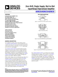
1 Precision, Low Noise, CMOS, rail -to- rail , Input/Output Operational AmplifiersData Sheet AD8605/AD8606/AD8608 Rev. O Document Feedback Information furnished by Analog Devices is believed to be accurate and reliable. However, no responsibility is assumed by Analog Devices for its use, nor for any infringements of patents or other rights of third parties that may result from its use. Specifications subject to change without notice. No license is granted by implication or otherwise under any patent or patent rights of Analog Devices. Trademarks and registered trademarks are the property of their respective owners. One Technology Way, Box 9106, Norwood, MA 02062-9106, : 2002 2017 Analog Devices, Inc. All rights reserved. Technical Support FEATURES Low offset voltage: 65 V maximum Low input bias currents: 1 pA maximum Low noise: 8 nV/ Hz Wide bandwidth: 10 MHz High open-loop gain: 1000 V/mV Unity gain stable Single-supply operation: V to V 5-ball WLCSP for single (AD8605) and 8-ball WLCSP for dual (AD8606) APPLICATIONS Photodiode amplification Battery-powered instrumentation Multipole filters Sensors Barcode scanners Audio GENERAL DESCRIPTION The AD8605, AD8606, and AD86081 are single, dual, and quad rail -to- rail input and output, single-supply amplifiers.
2 They feature very low offset voltage, low input voltage and current noise, and wide signal bandwidth. They use the Analog Devices, Inc. patented DigiTrim trimming technique, which achieves superior precision without laser trimming. The combination of low offsets, low noise, very low input bias currents, and high speed makes these amplifiers useful in a wide variety of applications. Filters, integrators, photodiode amplifiers, and high impedance sensors all benefit from the combination of performance features. Audio and other ac applications benefit from the wide bandwidth and low distortion. Applications for these amplifiers include optical control loops, portable and loop-powered instrumentation, and audio amplification for portable devices. The AD8605, AD8606, and AD8608 are specified over the extended industrial temperature range ( 40 C to +125 C). Th e AD8605 single is available in 5-lead SOT-23 and 5-ball WLCSP packages.
3 The AD8606 dual is available in an 8-lead MSOP, an 8-ball WLSCP, and a narrow SOIC surface-mounted package. The AD8608 quad is available in a 14-lead TSSOP package and a narrow 14-lead SOIC package. The 5-ball and 8-ball WLCSP offer the smallest available footprint for any surface-mounted operational amplifier. The WLCSP, SOT-23, MSOP, and TSSOP versions are available in tape-and-reel only. 1 Protected by Patent No. 5,969,657. PIN CONFIGURATIONS 12354 IN+INV+OUTAD8605 TOP VIEW(Not to Scale)V 02731-00102731-057 TOP VIEW(BALL SIDE DOWN)BALLA1 CORNERA1A2A3B1B3C1C2C3AD8606+INAV +INB INA INBOUTAV+OUTBF igure 1. 5-Lead SOT-23 (RJ Suffix) Figure 2. 8-Ball WLCSP (CB Suffix) AD8605 ONLYOUTV+V +IN IN13542 TOP VIEW(BUMP SIDE DOWN)02731-006 IN A+IN AV++IN B IN BOUT BOUT D IN D+IN DV +IN C IN COUT COUT A123456714131211109802731-004AD8608 TOP VIEW(Not to Scale)Figure 3. 5-Ball WLCSP (CB Suffix) Figure 4.
4 14-Lead SOIC_N (R Suffix) IN A+IN AV OUT B IN B+IN BV+18 OUT A4502731-003AD8606 TOP VIEW(Not to Scale)OUT A IN A+IN AV++IN B IN BOUT B IN D+IN DV OUT D IN COUT C+IN C1481702731-002AD8608 TOP VIEW(Not to Scale)Figure 5. 8-Lead MSOP (RM Suffix), 8-Lead SOIC_N (R Suffix) Figure 6. 14-Lead TSSOP (RU Suffix) AD8605/AD8606/AD8608 Data Sheet Rev. O | Page 2 of 24 TABLE OF CONTENTS Features .. 1 Applications .. 1 General Description .. 1 Pin Configurations .. 1 Revision History .. 2 5 V Electrical Specifications .. 4 V Electrical Specifications .. 6 Absolute Maximum Ratings .. 8 ESD Caution .. 8 Typical Performance Characteristics .. 9 Applications Information .. 16 Output Phase Reversal .. 16 Maximum Power Dissipation .. 16 Input Overvoltage Protection .. 16 THD + Noise .. 16 Total Noise Including Source Resistors .. 17 Channel Separation .. 17 Capacitive Load Drive .. 17 Light Sensitivity.
5 18 WLCSP Assembly Considerations .. 18 I- V Conversion Applications .. 19 Photodiode Preamplifier Applications .. 19 Audio and PDA Applications .. 19 Instrumentation Amplifiers .. 20 DAC Conversion .. 20 Outline Dimensions .. 21 Ordering Guide .. 24 REVISION HISTORY11/2017 Rev. N to Rev. O Added Figure 44 and Figure 45; Renumbered Sequentially .. 15 Changes to Figure 51 .. 17 Changes to Ordering Guide .. 24 4/ 2013 Rev. M to Rev. N Changes to Input Overvoltage Section and THD + Noise Section .. 16 Changes to Total Noise Including Source Resistors Section .. 17 Updated Outline Dimensions .. 24 2/ 2013 Rev. L to Rev. M Updated Outline Dimensions .. 21 Changes to Ordering Guide .. 24 2/ 2012 Rev. K to Rev. L Changed Functional B lock Diagrams Section to Pin Configuration Section .. 1 Changes to Figure 11 .. 9 Added Figure 33 .. 13 8/2011 Rev. J to Rev. K Changes to Figure 20.
6 2 Updated Outline Dimensions .. 20 Changes to Ordering Guide .. 23 8/2010 Rev. I to Rev. J Changes to Figure 10 and Figure 11 .. 9 Changes to Figure 15 .. 10 Changes to Figure 36 .. 13 Changes to Figure 42 .. 14 Updated Outline Dimensions .. 20 Changes to Ordering Guide .. 23 9/2008 Rev. H to Rev. I Changes to Input Overvoltage Protection 15 Changes to Ordering Guide .. 22 2/2008 Rev. G to Rev. H Changes to Features .. 1 Changes to Table 1 .. 4 Changes to Table 2 .. 6 Changes to Figure 11 .. 9 Changes to Figure 13, Figure 14, and Figure 16 Captions .. 10 Changes to Figure 15, Figure 17, and Figure 18 .. 10 Changes to Figure 34 and Figure 35 Captions .. 13 Changes to Figure 36 .. 13 Changes to Figure 37 Caption .. 14 Changes to Figure 38 and Figure 41 .. 14 Changes to Figure 45 .. 15 Changes to Audio and PDA Applications Section .. 18 Changes to Figure 52 .. 18 Changes to Ordering Guide.
7 22 10/2007 Rev. F to Rev. G Changes to Figure 2 .. 1 Updated Outline Dimensions .. 20 8/ 2007 Rev. E to Rev. F Added 8-Ball WLCSP Package .. Universal Changes to Features .. 1 Changes to Ta b l e 1 .. 3 Changes to Table 2 .. 5 Changes to Table 4 .. 7 Updated Outline Dimensions .. 19 Changes to Ordering Guide .. 21 Data Sheet AD8605/AD8606/AD8608 Rev. O | Page 3 of 24 1/2006 Rev. D to Rev. E Changes to Table 1 .. 3 Changes to Table 2 .. 5 Changes to Table 4 .. 6 Changes to Figure 12 Caption .. 8 Changes to Figure 26 and Figure 27 11 Changes to Figure 33 Caption .. 12 Changes to Figure 44 .. 14 Updated Outline Dimensions .. 19 Changes to Ordering Guide .. 20 5/2004 Rev. C to Rev. D Updated Universal Edit to Light Sensitivity Section .. 16 Updated Outline Dimensions .. 19 Changes to Ordering Guide .. 20 7/2003 Rev. B to Rev. C Changes to Features .. 1 Change to General Description.
8 1 Addition to Functional Block Diagrams .. 1 Addition to Absolute Maximum Ratings .. 4 Addition to Ordering Guide .. 4 Change to Equation in Maximum Power Dissipation Section .. 11 Added Light Sensitivity Section .. 12 Added New Figure 8; Renumbered Subsequently .. 13 Added New MicroCSP Assembly Considerations Section .. 13 Changes to Figure 9 .. 13 Change to Equation in Photodiode Preamplifier Applications Section .. 13 Changes to Figure 12 .. 14 Change to Equation in D/A Conversion Section .. 14 Updated Outline Dimensions .. 15 3/2003 Rev. A to Rev. B Changes to Functional Block Diagram .. 1 Changes to Absolute Maximum 4 Changes to Ordering Guide .. 4 Changes to Figure 9 .. 13 Updated Outline 15 11/2002 Rev. 0 to Rev. A Change to Electrical Characteristics .. 2 Changes to Absolute Maximum 4 Changes to Ordering Guide .. 4 Change to TPC 6 .. 5 Updated Outline 15 5/2002 Revision 0: Initial Version AD8605/AD8606/AD8608 Data Sheet Rev.
9 O | Page 4 of 24 5 V ELECTRICAL SPECIFICATIONS VS = 5 V, VCM = VS/2, TA = 25 C, unless otherwise noted. Table 1. Parameter Symbol Conditions Min Typ Max Unit INPUT CHARACTERISTICS Offset Voltage VOS AD8605/AD8606 (Except WLCSP) VS = V, VCM = 3 V 20 65 V AD8608 VS = V, VCM = V 20 75 V AD8605/AD8606/AD8608 VS = 5 V, VCM = 0 V to 5 V 80 300 V 40 C < TA < +125 C 750 V Input Bias Current IB 1 pA AD8605/AD8606 40 C < TA < +85 C 50 pA AD8605/AD8606 40 C < TA < +125 C 250 pA AD8608 40 C < TA < +85 C 100 pA AD8608 40 C < TA < +125 C 300 pA Input Offset Current IOS pA 40 C < TA < +85 C 20 pA 40 C < TA < +125 C 75 pA Input Voltage Range 0 5 V Common-Mode Rejection Ratio CMRR VCM = 0 V to 5 V 85 100 dB 40 C < TA < +125 C 75 90 dB Large Signal Voltage Gain AVO RL = 2 k , VO = V to V 300 1000 V/mV Offset Voltage Drift AD8605/AD8606 VOS/ T 40 C < TA < +125 C 1 V/ C AD8608 VOS/ T 40 C < TA < +125 C V/ C INPUT CAPACITANCE Common-Mode Input Capacitance CCOM pF Differential Input Capacitance CDIFF pF OUTPUT CHARACTERISTICS Output Voltage High VOH IL = 1 mA V IL = 10 mA V 40 C < TA < +125 C V Output Voltage Low VOL IL = 1 mA 20 40 mV IL= 10 mA 170 210 mV 40 C < TA < +125 C 290 mV Output Current IOUT 80 mA Closed-Loop Output Impedance ZOUT f = 1 MHz.
10 AV = 1 1 POWER SUPPLY Power Supply Rejection Ratio PSRR AD8605/AD8606 VS = V to V 80 95 dB AD8605/AD8606 WLCSP VS = V to V 75 92 dB AD8608 VS = V to V 77 92 dB 40 C < TA < +125 C 70 90 dB Supply Current/Amplifier ISY IOUT = 0 mA 1 mA 40 C < TA < +125 C mA DYNAMIC PERFORMANCE Slew Rate SR RL = 2 k , CL = 16 pF 5 V/ s Settling Time tS To , 0 V to 2 V step, AV = 1 <1 s Unity Gain Bandwidth Product GBP 10 MHz Phase Margin M 65 Degrees Data Sheet AD8605/AD8606/AD8608 Rev. O | Page 5 of 24 Parameter Symbol Conditions Min Typ Max Unit NOISE PERFORMANCE Peak-to-Peak Noise en p-p f = Hz to 10 Hz V p-p Voltage Noise Density en f = 1 kHz 8 12 nV/ Hz en f = 10 kHz nV/ Hz Current Noise Density in f = 1 kHz pA/ Hz AD8605/AD8606/AD8608 Data Sheet Rev. O | Page 6 of 24 V ELECTRICAL SPECIFICATIONS VS = V, VCM = VS/2, TA = 25 C, unless otherwise noted.
