Transcription of Precision, Ultralow Noise, RRIO, Zero-Drift Op Amp Data ...
1 Precision, Ultralow Noise, RRIO, Zero-Drift Op Amp data Sheet ada4528 -1/ ada4528 -2 Rev. F Document Feedback Information furnished by Analog Devices is believed to be accurate and reliable. However, no responsibility is assumed by Analog Devices for its use, nor for any infringements of patents or other rights of third parties that may result from its use. Specifications subject to change without notice. No license is granted by implication or otherwise under any patent or patent rights of Analog Devices. Tra demarks and registered trademarks are the property of their respective owners.
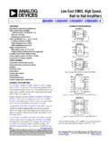
2 One Technology Way, Box 9106, Norwood, MA 02062-9106, Tel: 2011 2017 Analog Devices, Inc. All rights reserved. Technical Support FEATURES Low offset voltage : V maximum Low offset voltage drift: V/ C maximum Low noise nV/ Hz at f = 1 kHz, AV = +100 97 nV p-p at f = Hz to 10 Hz, AV = +100 Open-loop gain: 130 dB minimum CMRR: 135 dB minimum PSRR: 130 dB minimum Unity-gain crossover: 4 MHz Gain bandwidth product: 3 MHz at AV = +100 3 dB closed-loop bandwidth: MHz Single-supply operation: V to V Dual-supply operation: V to V Rail-to-rail input and output Unity-gain stable APPLICATIONS Thermocouple/thermopile Load cell and bridge transducers Precision instrumentation Electronic scales Medical instrumentation Handheld test equipment GENERAL DESCRIPTION The ada4528 -1/ ada4528 -2 are Ultralow noise, Zero-Drift operational amplifiers featuring rail-to -rail input and output swing.
3 With an offset voltage of V, offset voltage drift of V/ C, and typical noise of 97 nV p-p ( Hz to 10 Hz, AV = +100), the ada4528 -1/ ada4528 -2 are well suited for applications in which error sources cannot be tolerated. The ada4528 -1/ ada4528 -2 have a wide operating supply range of V to V, high gain, and excellent CMRR and PSRR specifi-cations, which make it ideal for applications that require precision amplification of low level signals, such as position and pressure sensors, strain gages, and medical instrumentation. The ada4528 -1/ ada4528 -2 are specified over the extended industrial temperature range ( 40 C to +125 C).
4 The ada4528 -1 and ada4528 -2 are available in 8-lead MSOP and 8-lead LFCSP packages. For more information about the ada4528 -1/ ada4528 -2, see the AN-1114 Application Note, Lowest Noise Zero-Drift Amplifier Has nV/ Hz voltage Noise Density. PIN CONNECTION DIAGRAMS NIC1 IN2+IN3V 4 NIC8V+7 OUT6 NIC5 NOTES1. NIC = NO INTERNAL VIEW(Not to Scale)09437-001 Figure 1. ada4528 -1 Pin Configuration, 8-Lead MSOP 09437-102 ada4528 -1 TOP VIEW(Not to Scale)3+IN4V 1 NIC2 IN6 OUT5 NIC8 NIC7V+NOTES1. NIC = NO INTERNAL CONNECT THE EXPOSED PAD TOV OR LEAVE IT UNCONNECTED. Figure 2. ada4528 -1 Pin Configuration, 8-Lead LFCSP For ada4528 -2 pin connections and for more information about the pin connections for these products, see the Pin Configurations and Function Descriptions section.
5 1101001101001k10k100k1M10 MVOLTAGE NOISE DENSITY (nV/ Hz)FREQUENCY (Hz)09437-063 VSY = 5 VVCM = VSY/2AV = 1 Figure 3. voltage Noise Density vs. Frequency Table 1. Analog Devices, Inc., Zero-Drift Op Amp Portfolio1 Type Ultralow Noise Micropower (<20 A) Low Power (<1 mA) 16 V Operating voltage 30 V Operating voltage Single ada4528 -1 ADA4051-1 AD8628 AD8638 ADA4638-1 AD8538 Dual ada4528 -2 ADA4051-2 AD8629 AD8639 AD8539 Quad AD8630 1 See for the latest selection of Zero-Drift operational amplifiers. ada4528 -1/ ada4528 -2 data Sheet Rev. F | Page 2 of 24 TABLE OF CONTENTS Features .. 1 Applications.
6 1 General Description .. 1 Pin Connection Diagrams .. 1 Revision History .. 2 Specifications .. 3 Electrical Characteristics V Operation .. 3 Electrical Characteristics 5 V Operation .. 4 Absolute Maximum Ratings .. 6 Thermal Resistance .. 6 ESD Caution .. 6 Pin Configurations and Function Descriptions ..7 Typical Performance Characteristics ..9 Applications Information .. 19 Input Protection .. 19 Rail-to -Rail Input and Output .. 19 Noise Considerations .. 19 Comparator Operation .. 21 Printed Circuit Board Layout .. 22 Outline Dimensions .. 23 Ordering Guide .. 24 REVISION HISTORY 8/2017 Rev. E to Rev. F Deleted CP-8-19.
7 Universal Updated Outline Dimensions .. 24 Changes to Ordering Guide .. 25 6/2017 R e v. D t o R e v. E Deleted CP-8-12 .. Universal Added CP-8-19 .. Universal Updated Outline Dimensions .. 24 Changes to Ordering Guide .. 25 5/ 2013 Rev. C to Rev. D Added 8-Lead LFCSP Package (CP-8-11) .. Universal Changes to Table 5 .. 7 Added Figure 7, Renumbered Sequentially .. 8 Added Figure 62 and Figure 63 .. 19 Changes to Comparator Operation Section, Figure 68, Figure 69, Figure 70, and Figure 71 .. 21 Changes to Figure 72 .. 22 Added Figure 76 .. 24 9/2012 Rev. B to Rev. C Changes to Features 1 Added Comparator Operation Section.
8 21 Added Figure 65 to Figure 69; Renumbered Sequentially .. 21 7/2012 Rev. A to Rev. B Added ada4528 -2 .. Universal Changes to Features Section, Figure 1, Figure 2, and Ta b l e 1 .. 1 Added Pin Connection Diagrams Section and Figure 3; Renumbered Sequentially .. 1 Changes to Table 2 .. 3 Changes to Table 3 .. 5 Change to Endnote 1 of Table 4 and Thermal Resistance Section .. 7 Added Pin Configurations and Function Descriptions Section, Figure 4, Figure 5, and Table 6 .. 8 Added Figure 6 and Table 7 .. 9 Changes to Input Protection Section .. 19 Changes to Source Resistance Section and Caption of Figure 63.
9 20 Changes to Residual voltage Ripple Section and Caption of Figure 64 .. 21 Changes to Ordering Guide .. 22 9/ 2011 R e v. 0 t o R e v. A Added 8-Lead LFCSP_WD Package .. Universal Changes to General Description Section .. 1 Added Figure 2; Renumbered Sequentially .. 1 Changes to offset voltage , offset voltage Drift, Power Supply Rejection Ratio, and Settling Time to Parameters, Ta b l e 2 .. 3 Changes to Thermal Resistance Section and Table 5 .. 5 Changes to Figure 41 and Figure 12 Changes to Figure 45 and Figure 13 Updated Outline Dimensions .. 18 Changes to Ordering Guide .. 18 1/2011 Revision 0: Initial Version data Sheet ada4528 -1/ ada4528 -2 Rev.
10 F | Page 3 of 24 SPECIFICATIONS ELECTRICAL CHARACTERISTICS V OPERATION VSY = V, VCM = VSY/2, TA = 25 C, unless otherwise specified. Table 2. Parameter Symbol Test Conditions/Comments Min Typ Max Unit INPUT CHARACTERISTICS offset voltage VOS VCM = 0 V to V V 40 C TA +125 C, MSOP package 4 V 40 C TA +125 C, LFCSP package V offset voltage Drift VOS/ T 40 C TA +125 C, MSOP package V/ C 40 C TA +125 C, LFCSP package V/ C Input Bias Current IB 220 400 pA 40 C TA +125 C 600 pA Input Offset Current IOS 440 800 pA 40 C TA +125 C 1 nA Input voltage Range 0 V Common-Mode Rejection Ratio CMRR VCM = 0 V to V 135 158 dB 40 C TA +125 C 116 dB Open-Loop Gain AVO RL = 10 k , VO = V to V 130 140 dB 40 C TA +125 C 126 dB ada4528 -1 RL = 2 k , VO = V to V 125 132 dB 40 C TA +125 C 121 dB ada4528 -2 RL = 2 k.
