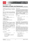
Transcription of PWM Control type DC/DC converter IC - Rohm
1 Datasheet AC/DC Drivers PWM Control type DC/DC converter IC. BM1P061FJ / BM1P062FJ / BM1P101FJ / BM1P102FJ. General Features The PWM type DC/DC converter (BM1 Pxxx) for PWM frequency : 65kHz, 100kHz AC/DC provides an optimum system for all products PWM current mode method that include an electrical outlet. Frequency Hopping function BM1 Pxxx supports both isolated and non-isolated Burst operation / Frequency reduction function devices, enabling simpler design of various types of when load is light low-power electrical converters. Built-in 650V start circuit BM1 Pxxx built in a HV starter circuit that tolerates VCC pin under voltage protection 650V, it contributes to low-power consumption. VCC pin over voltage protection With switching MOSFET and current detection CS pin Open protection resistors as external devices, a higher degree of CS pin Leading-Edge-Blanking function design freedom is achieved.
2 Switching frequency Per-cycle over current protection circuit adopts fixed system. Since current mode Control is Current protection with AC voltage compensation utilized, current is restricted in each cycle and Soft start excellent performance is demonstrated in bandwidth Secondary Over current protection circuit and transient response. At light load, the switching frequency is reduced and high efficiency is achieved. A frequency hopping function is also on chip, which Package contributes to low EMI. SOP-J8 Pitch BM1 Pxxx also has built-in function such as soft start, (Typ) (Typ) (Typ) (Typ). burst mode, over current limiter per cycle, VCC over voltage protection and over load protection. Basic specifications Operating Power Supply Voltage Range: VCC to VH to 600V.
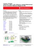
3 Operating Current: Normal Mode (Typ) Applications Burst Mode (Typ) AC adapters and household appliances (vacuum Oscillation Frequency: BM1P06xFJ 65kHz (Typ) cleaners, humidifiers, air cleaners, air conditioners, IH. BM1P10xFJ 100kHz (Typ) cooking heaters, rice cookers, etc. Operating Temperature: - 40deg. to +105 . Application circuit Line-Up Frequency VCCOVP. BM1P101FJ 100kHz Auto Restart BM1P102FJ 100kHz Latch BM1P061FJ 65kHz Auto Restart BM1P062FJ 65kHz Latch Figure 1 Application circuit Product structure Silicon monolithic integrated circuit This product is not designed protection against radioactive rays . 2012 ROHM Co., Ltd. All rights reserved. TSZ02201-0F2F0A200090-1-2. 1/19. TSZ22111 15 001 BM1P061FJ / BM1P062FJ / BM1P101FJ / BM1P102FJ Datasheet Absolute Maximum Ratings Ta=25 C.)
4 Parameter Symbol Rating Unit Conditions Maximum voltage 1 Vmax1 V VCC. Maximum voltage 2 Vmax2 V CS, FB, ACMONI. Maximum voltage 3 Vmax3 V OUT. Maximum voltage 4 Vmax4 650 V VH. OUT Pin Peak Current IOUT A. Allowable dissipation Pd (Note1) W When implemented Operating o Topr -40 +105 C. temperature range o MAX junction temperature Tjmax 150 C. Storage o Tstr -55 +150 C. temperature range (Note1) When mounted (on 70 mm 70 mm, mm thick, glass epoxy on single-layer substrate). Reduce to mW/ C when Ta = 25 C or above. Caution: Operating the IC over the absolute maximum ratings may damage the IC. The damage can either be a short circuit between pins or an open circuit between pins and the internal circuitry.
5 Therefore, it is important to consider circuit protection measures, such as adding a fuse, in case the IC is operated over the absolute maximum ratings. Operating Conditions Ta=25 C . Parameter Symbol Rating Unit Conditions Power supply voltage range 1 VCC V VCC pin voltage Power supply voltage range 2 VH 80 600 V VH pin voltage Electrical Characteristics (Unless otherwise noted, Ta = 25 C, VCC = 15 V). Specifications Parameter Symbol Unit Conditions Minimum Standard Maximum [Circuit current]. VCC= Circuit current (STBY) ISTBY - 12 20 A. detecting VCCUVLO . FB= Circuit current (ON) 1 ION1 - 600 1000 A. (during pulse operation). FB= Circuit current (ON) 2 ION2 - 350 450 A. (during burst operation).
6 [VCC protection function]. VCC UVLO voltage 1 VUVLO1 V VCC rise VCC UVLO voltage 2 VUVLO2 V VCC drop VCC UVLO hysteresis VUVLO3 - - V VUVLO3= VUVLO1- VUVLO2. Start up circuit operation VCC Recharge start voltage VCHG1 V. voltage VCC Recharge stop voltage VCHG2 V The stop voltage from VCHG1. VCC OVP voltage 1 VOVP1 V VCC rise VCC drop VCC OVP voltage 2 VOVP2 V. BM1P061FJ/BM1P101FJ. VCC OVP hysteresis VOVP3 - - V BM1P061FJ/BM1P101FJ. [OUT pin]. OUT Pin High voltage VOUTH V IO=-20mA. OUT Pin Low voltage VOUTL - - V IO=+20mA. OUT Pin pull down resistance RPDOUT 75 100 125 k . [ ACMONI Detector ]. ACMONI detect voltage1 VACMONI1 V ACMONI rise ACMONI detect voltage2 VACMONI2 V ACMONI drop ACMONI hysteresis VACMONI3 V.
7 ACMONI Timer TACMONI1 180 256 330 mS. [Start circuit block ]. Start current 1 ISTART1 mA VCC= 0V. Start current 2 ISTART2 mA VCC=10V. Inflow current from VH pin OFF current ISTART3 - 10 20 uA. after UVLO released UVLO. Start current changing voltage VSC V. 2012 ROHM Co., Ltd. All rights reserved. TSZ02201-0F2F0A200090-1-2. 2/19. TSZ22111 15 001 BM1P061FJ / BM1P062FJ / BM1P101FJ / BM1P102FJ Datasheet Electrical Characteristics (Unless otherwise noted, Ta = 25 C, VCC = 15 V). Specifications Parameter Symbol Unit Conditions Minimum Standard Maximum [PWM type DCDC driver block]. FB= Oscillation frequency 1a FSW1a 60 65 70 kHz average frequency BM1P061FJ/BM1P062FJ. FB= Oscillation frequency 1b FSW1b 90 100 110 kHz average frequency BM1P101FJ/BM1P102FJ.
8 FB= Oscillation frequency 2 FSW2 - 25 - kHz average frequency FB= Hopping fluctuation FDEL1 - - kHz average frequency frequency range 1. BM1P061FJ/BM1P062FJ. FB= Hopping fluctuation FDEL2 - - kHz average frequency frequency range 2. BM1P101FJ/BM1P102FJ. Hopping fluctuation frequency FCH 75 125 175 Hz Minimum pulse width Tmin - 400 - ns Soft start time 1 TSS1 ms Soft start time 2 TSS2 ms Soft start time 3 TSS3 ms Soft start time 4 TSS4 ms Maximum duty Dmax %. FB pin pull-up resistance RFB 22 30 38 k . FB / CS gain Gain - - V/V. FB burst voltage 1 VBST1 V FB drop FB burst voltage 2 VBST2 V FB rise When overload is detected FB OLP voltage 1a VFOLP1A V. (FB rise). When overload is detected FB OLP voltage 1b VFOLP1B - - V.
9 (FB drop). FB OLP ON timer TFOLP 44 64 84 ms FB OLP Start up timer TFOLP2 26 32 38 ms FB OLP OFF timer TOLPST 358 512 666 ms VCC Pin voltage Latch released VCC voltage VLATCH - - V. BM1P062FJ/BM1P102FJ. VCCOVP. Latch mask time TLATCH 50 100 200 us BM1P062FJ/BM1P102FJ. [Over current detection block]. Over current detection voltage VCS V Ton=0us Over current detection VCS_SS1 - - V 0[ms] ~ TSS1[ms]. voltage SS1. Over current detection VCS_SS2 - - V TSS1 [ms] ~ TSS2 [ms]. voltage SS2. Over current detection VCS_SS3 - - V TSS2 [ms] ~ TSS3[ms]. voltage SS3. Over current detection VCS_SS4 - - V TSS3 [ms] ~ TSS4 [ms]. voltage SS4. Leading Edge Blanking Time TLEB - 250 - ns Over current detection AC.
10 KCS 12 20 28 mV/us Voltage compensation factor 2012 ROHM Co., Ltd. All rights reserved. TSZ02201-0F2F0A200090-1-2. 3/19. TSZ22111 15 001 BM1P061FJ / BM1P062FJ / BM1P101FJ / BM1P102FJ Datasheet PIN DESCRIPTIONS. Table 1. Pin Description ESD Diode NO. Pin Name I/O Function VCC GND. 1 ACMONI I Comparator input pin . 2 FB I Feedback signal input pin . 3 CS I Primary Current sense pin . 4 GND I/O GND pin - 5 OUT O External MOSFET driver pin . 6 VCC I/O Power supply input pin - . 7 - Non Connection - - 8 VH I Starter pin - . I/O Equivalent Circuit Diagram Figure 2 . I/O Equivalent Circuit Diagram 2012 ROHM Co., Ltd. All rights reserved. TSZ02201-0F2F0A200090-1-2. 4/19. TSZ22111 15 001 BM1P061FJ / BM1P062FJ / BM1P101FJ / BM1P102FJ Datasheet Block Diagram +.