Transcription of Re-designing normally-on load switches with zero …
1 Re-designing normally -on load switches with zero-power MOSFETs reduces power consumption By Bob Chao and Linden Harrison Advanced Linear Devices As circuit supply voltages decrease and green energy trends grow in popularity, designers should re-examine some of the circuits that continually consume power in an effort to reduce overall system power consumption. One circuit that requires continuous voltage is the normally -ON . circuit and it is now possible to redesign this circuit with new components to reduce wasted energy. Low voltage operation and ultra-low power consumption have become increasingly important as circuit supply voltages decrease. Today's portable consumer electronic designs conserve battery power and minimize battery drain by temporarily turning off unused parts of a system by using a high-side load switch. load switches are usually processor-controlled, and therefore must be CMOS-compatible.
2 Power MOSFETs have become the primary switching element for high-side load switch applications, and optimum performance is achieved when using a P-channel device. Many of these circuits are known as normally -OFF circuits, meaning they require the power supply to be on in order to operate. Increasingly, there is a trend to re-examine high-side load switches as one of the generally- accepted, facts-of-life type of circuits. Where conventional wisdom and tradition determine a way to build traditional circuits, high-side load switches are wasteful of energy. However, these circuits were tolerated because they wasted only small amounts of energy at a time. New green trends call for improvements in the efficiency of these types of applications by many orders of magnitude. Often this can be accomplished at incremental or no additional cost and economical payback can be achieved across the operating life of the system.
3 Recently, re-design efforts have boosted the energy efficiency of compact florescent lamps (CPL) and small wall-powered modules used for everything from battery chargers and cell phones to printer adapters. A large group of circuits that work in reverse to these normally -OFF circuits are known as normally -ON circuits. They are required to be on without power and off when actually working, or powered. A burglar alarm or an emergency alarm requiring the system to be in a normally -ON state is an example of such a system. These systems will activate and send a signal only when the normally -ON status is interrupted. These types of circuits are continuously on for 24 hours a day and normally sit idle, waiting for an event to happen that will disconnect its on . status, allowing it to jump into action. Sometimes, this class of circuits is also known as very low duty cycle circuits, where their off time is very low compared to their on time.
4 For these circuits, the ON time power consumption can become an issue, because they are doing nothing when they are on while monitoring for an external event to take place. During this ON state, AC or battery power is being consumed. This is a class of circuits that is normally -ON but requires only very low incidence of OFF-state. This situation creates the need for a normally -ON load switch, and one that simultaneously consumes zero- power. Such a switch requires a depletion-mode MOSFET, which acts like a normally -closed . SPST relay. In the past, the electronic industry has typically designed this type of circuit by using more power from an AC source in order to build a circuit that performs and emulates this required function. An emergency light design provides an example of a normally -OFF circuit that continually uses power. Typically an AC power module is connected to an AC power source 24/7 and burns a small amount of AC power.
5 This power is supplied to a circuit that may employ a normally -closed . SPST relay. This relay is energized continuously until the AC power source is interrupted, then the SPST relay is opened and switched to a backup battery pack to power an emergency light or an alarm. The AC power module is always on and must be able to supply enough voltage and current to switch this SPST relay properly. This usually consumes several watts of AC power continuously just to enable this emergency light module. The actual design requirement, in this case, is just to turn on a power MOSFET to switch on the backup battery circuit only when the emergency module looses AC power. During the rest of the time, the design wants to burn zero power. This is when a depletion-mode MOSFET and an enhancement-mode power MOSFET can work together to achieve zero power and robust current-driving load switch.
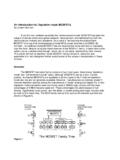
6 A depletion-mode MOSFET's channel is conductive and its drain current ID(on) flows when the gate terminal is at zero volts (VGS = 0V), it requires no gate voltage to function. ( Vgs can even be several volts positive). Applying an increasingly negative bias at the gate reduces conduction in the channel until finally its threshold voltage (-VTH) is reached, and conduction ceases. Advanced Linear Devices' depletion-mode EPAD products (ALD1148xx and ALD1149xx series) are low- voltage, precision-matched dual/quad N-channel devices with ultra-low threshold voltages categorized in several values over a range from to The circuit shown in Figure 1 operates so that with 0V on the gate of Q1 (an ALD114904), the device is on. Its on-state resistance RDS(on) is about 5-K , which together with bias resistor R3. forms a resistive divider. As a result the gate of the P-channel power MOSFET Q2 is pulled low, turning it on and so activating the load .
7 If Q1's gate is now pulled increasingly negative, it will reduce conduction until finally -V(TH) is reached. This will cause the gate of Q2 to go high and switch off, de-activating the load . Figure 1. The supply voltage for this low-voltage circuit can typically range from about + to + , and will typically switch on/off in less than 100-nS. This load switch can easily source > 3A of output current if required. Because the quiescent current for the circuit results only from leakage currents of the two transistors (<100-nA ) - it can therefore be considered to consume zero power. As the ALD and I-R devices are both duals , a normally -on DOUBLE-pole version of this circuit can be easily created. The input terminals to the circuit can either be connected together to provide a DPST. action, or left independent to form two SPST switches . To create a normally -on circuit with zero power and the load to be normally -off, replace the P-channel load driver IRF7325 with an N- channel load driver such as IRF7313.
8 In this case, the circuit is normally -on and the load is normally -off, and the entire circuit only consume leakage currents. As compared to a relay activated circuit, quiescent power consumption in this circuit is down by several orders of magnitude, from a few watts to a few microwatts. A very unique normally -on, high-side SPST switch circuit is shown in Figure 2, which shows an ultra low-power switch using an ALD110900A. Advanced Linear Devices' ALD110800 (quad) and ALD110900 (dual) EPAD devices are totally unique MOSFET products, because they have a true "zero-threshold" voltage. This makes them both enhancement-mode AND depletion-mode devices. When the gate is set at , the drain current = 1 A @ VDS = , which provides a type of circuit with an output voltage level biased at or near the input voltage level, but without any voltage level shift. Here the zero-threshold transistor Q2 is normally conducting when its gate is high.
9 When enhancement-mode EPAD transistor Q1's gate is made high, its drain goes low, thus turning off Q2. and de-energizing the load . Note the supply is below even the threshold voltage of most of today's MOSFETs. Figure 2. Summary Increasingly, electronic designers realize that a small amount of wasted power multiplied millions of times in circuits running 24 hours a day contributes greatly to wasted energy. Drastically reducing energy waste can be achieved by adopting new circuits that utilize some of the latest components. Zero power normally -ON load switch designs utilizing a combination of an ultra-low power depletion-mode MOSFET and an enhancement-mode power MOSFET is one way that can save cost, space and wasted energy.