Transcription of (Saturated) MOSFET Small-Signal Model Transconductance
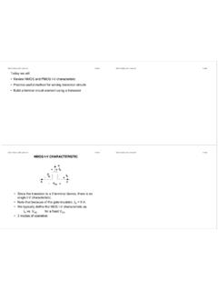
1 11. (Saturated) MOSFET Small-Signal Model Transconductance Concept: find an equivalent circuit which interrelates the incremental changes The Small-Signal drain current due to vgs is therefore given by in iD, vGS, vDS, etc. for the MOSFET in saturation id = gm vgs. vGS = VGS + vgs , iD = ID + id -- we want to find id = (?) vgs D iD = ID + id G. We have the functional dependence of the total drain current in saturation: +. +. B VDS = 4 V. vgs _. iD = n Cox (W/2L) (vGS - VTn ) (1 + nvDS) = iD(vGS, vDS). 2. _. + S. Solution: do a Taylor expansion around the DC operating point (also called the VGS = 3 V_. quiescent point or Q point) defined by the DC voltages Q(VGS, VDS): 2 600. i D 1 iD 2. iD = ID + ( v gs ) + --- ( v gs ) + . v GS 2 v2 500. id vGS = VGS + vgs Q GS. Q iD 400. Q vGS = VGS = 3 V. ( A) 300. If the Small-Signal voltage is really small, then we can neglect all everything past gm = id / vgs the linear term -- 200.
2 100. i D. iD = ID + ( v gs ) = I D + g m v gs v GS. 1 2 3 4 5 6. Q VDS (V). where the partial derivative is defined as the Transconductance , gm. EE 105 fall 1998 EE 105 fall 1998. Lecture 11 Lecture 11. Another View of gm Transconductance (cont.). * Plot the drain current as a function of the gate-source voltage, so that Evaluating the partial derivative: the slope can be identified with the Transconductance : g m = n C ox ----- ( V GS V Tn ) ( 1 + n V DS ). W. L. D iD = ID + id G. + In order to find a simple expression that highlights the dependence of gm on the + B VDS = 4 V. vgs _ DC drain current, we neglect the (usually) small error in writing: _. + S. VGS = 3 V_. 2I D. 2 n C ox ----- I D = -------------------------- W. gm =. L V GS V Tn iD(vGS, VDS = 4 V). 600. 500 For typical values (W/L) = 10, ID = 100 A, and nCox = 50 AV-2 we find that id gm = id / vgs iD 400 Q. ( A) 300. gm = 320 AV-1 = mS. 200. 100.
3 1 2 3 4 5 6 vGS (V). vGS = VGS = 3 V vGS = VGS + vgs EE 105 fall 1998 EE 105 fall 1998. Lecture 11 Lecture 11. (Partial) Small-Signal Circuit Model Output Conductance/Resistance How do we make a circuit which expresses id = gm vgs ? Since the current is not We can also find the change in drain current due to an increment in the drain- across its controlling voltage, we need a voltage-controlled current source: source voltage: i D. g o = ------------ = n C ox ------ ( V GS V Tn ) n n I D. W 2. v DS 2L. Q. gate id The output resistance is the inverse of the output conductance + drain vgs gmvgs _ source 1 1. r o = ----- = ------------ _ go n ID. The (partial) Small-Signal circuit Model with ro added looks like: id = gm vgs + (1/ro)vds gate drain + +. id gmvgs ro vds vgs _ source _. EE 105 fall 1998 EE 105 fall 1998. Lecture 11 Lecture 11. ,, MOSFET Capacitances in Saturation Complete Small-Signal Model fringe electric field lines gate All these capacitances are patched onto the Small-Signal circuit schematic source drain ,,, ,, ,,,, containing gm and ro.
4 Gmb is open-circuited for EECS 105 since vbs = 0 V. n+ n+. Csb qN (vGS) depletion Cdb overlap LD overlap LD region Cgd id gate + drain vgs Cgs Cgb gmvgs gmbvbs ro _ source _. vbs Csb Cdb +. bulk In saturation, the gate-source capacitance contains two terms, one due to the channel charge's dependence on vGS [(2/3)WLCox] and one due to the overlap of gate and source (WCov, where Cov is the overlap capacitance in fF per m of gate width). 2. C gs = --- WLC ox + WC ov 3. In addition, there is the small but very important gate-drain capacitance (just the overlap capacitance Cgd = Cov). There are depletion capacitances between the drain and bulk (Cdb) and between source and bulk (Csb). Finally, the extension of the gate over the field oxide leads to a small gate-bulk capacitance Cgb. EE 105 fall 1998 EE 105 fall 1998. Lecture 11 Lecture 11. p-channel MOSFETs p-channel MOSFET Models Structure is complementary to the n-channel MOSFET DC drain current in the three operating regions: -ID > 0.
5 , , In a CMOS technology, one or the other type of MOSFET is built into a well -- a deep diffused region -- so that there are electrically isolated bulk regions in the ID = 0 A ( V SG V T ). same substrate I D = p C ox ( W L )[ VSG + V Tp ( V SD 2 ) ] ( 1 + p V SD )VSD ( V SG V Tp, VSD VSG + V Tp ). 2. I D = p C ox ( W ( 2L ) ) ( V SG + V T p ) ( 1 + p VSD ) ( V SG V Tp, VSD VSG + V Tp ). , .. , . ,,,,,,,,,, ,,,,,,, ,, ,, The threshold voltage with backgate effect is given by: , n-channel p-channel V Tp = V TOp p ( ( V SB + 2 n ) 2 n ). ,,,,,,,,,,, , ,,,,,,, , MOSFET MOSFET . , Numerical values: , , , ,,,,,, ,,,,,,,,, ,,,,, pCox is a measured parameter. Typical value: pCox = 25 AV-2. ,,,,, A A. 1. mV. p -------------------------- L. (a). common bulk contact for isolated bulk contact with VTp = to V, which should be approximately -VTn for a well-controlled all n-channel MOSFETs p-channel MOSFET CMOS process (to ground or to the supply) shorted to source ,,,,,, ,,,, ,,,, ,,, ,, ,,, ,, ,,, ,, , p+ n+ source n+ drain p+ drain p+ source n+.
6 P-type substrate n well (b). EE 105 fall 1998 EE 105 fall 1998. Lecture 11 Lecture 11. p-channel MOSFET Small-Signal Model the source is the highest potential and is located at the top of the schematic source +. Cgs gmvsg gmbvsb ro vsg Cgd id vsb _ gate drain Cgb Csb Cdb _ bulk EE 105 fall 1998. Lecture 11.