Transcription of SERIES: PDS1-M DESCRIPTION: DC-DC CONVERTER
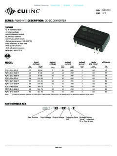
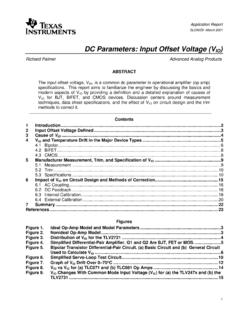
1 Of 8 SERIES: PDS1-M DESCRIPTION: DC-DC CONVERTER10/27/2022datepage1 of 8 FEATURES 1 W isolated output smaller package single and dual unregulated outputs 1,500 Vdc isolation short circuit protection extended temperature range (-40~105 C) antistatic protection up to 8kV high efficiency at light load efficiency up to 82%MODEL inputvoltageoutputvoltageoutputcurrentou tputpowerripple and noise2efficiencytyp(Vdc)range(Vdc)(Vdc)m in(mA)max(mA)max(W)typ(mVp-p)typ(%) ~ ~ ~ 5 10 ~ 12 5 ~ 15 3 ~ ~ ~ ~ ~ ~ ~ 5 10 ~ 9 6 ~ 12 5 ~ 15 3 ~ 24 2 ~ ~ ~ ~ ~ ~ 5 10 ~ 9 6 ~ 12 5 ~ 15 3 ~ 24 2 ~ : 1.
2 UL approved 2. Ripple and noise are measured at 20 MHz BW by parallel cable method with 1 F ceramic and 10 F electrolytic capacitors on the Resources: Product Page | 3D Model | PCB Inc SERIES: PDS1-M DESCRIPTION: DC-DC CONVERTER date 10/27/2022 page 2 of 8 input parameterconditions/descriptionmintypmax unitsoperating input Vdc input models5 Vdc input models12 Vdc input models15 Vdc input models24 Vdc input voltagefor maximum of 1 Vdc input models5 Vdc input models12 Vdc input models15 Vdc input models24 Vdc input filterOUTPUT parameterconditions/descriptionmintypmax unitsline regulationfor Vin change of 1% Vdc output modelsall other models regulationmeasured from 10% load to full Vdc output
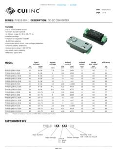
3 Models5 Vdc output models9 Vdc output models12 Vdc output models15 Vdc output models24 Vdc output models18128765%%%%%%voltage accuracysee tolerance envelope curveswitching frequency100% load, nominal input voltage 100kHztemperature coefficient100% load CPDS1 - SXX - XXX - M - XInput VoltageOutput VoltageOutputS = singleD = dualBase NumberPackaging StyleSMTP ackage Options"blank" = standardTR = Tape & ReelMODEL(CONTINUED)inputvoltageoutputvo ltageoutputcurrentoutputpowerripple and noise2efficiencytyp(Vdc)range(Vdc)(Vdc)m in(mA)max(mA)max(W)typ(mVp-p)typ(%) ~ ~ ~ ~ ~ ~ 5 10 ~ 9 6 ~ 12 5 ~ 15 3 ~ 24 2 2116080 Notes: 1.
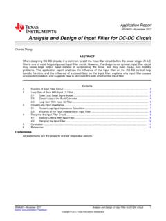
4 UL approved 2. Ripple and noise are measured at 20 MHz BW by parallel cable method with 1 F ceramic and 10 F electrolytic capacitors on the NUMBER KEYA dditional Resources: Product Page | 3D Model | PCB Inc SERIES: PDS1-M DESCRIPTION: DC-DC CONVERTER date 10/27/2022 page 3 of 8050100150200250 Time(sec.)Temperature( ) 245 (Max.)24521760 Max(>217)Sec C C CPROTECTIONS parameterconditions/descriptionmintypmax unitsshort circuit protection13 & 24 Vdc input modelsPDS1-S5-S12-M, PDS1-S5-D24-Mall other models: automatic recovery11ssNote: 1.
5 The supply voltage must be discontinued at the end of the short circuit durationSAFETY AND COMPLIANCE parameterconditions/descriptionmintypmax unitsisolation voltageinput to output for 1 minute at 1 mA ,500 Vdcisolation resistanceinput to output at 500 Vdc1,000M isolation capacitanceinput to output at 100 V20pFsafety approvals2certified to 60950-1: ULdesigned to meet 62368: ENconducted emissionsCISPR32/EN55032, class B (external circuit required, see Figure 1) radiated emissionsCISPR32/EN55032, class B (external circuit required, see Figure 1) ESDIEC/EN 61000-4-2, class B, contact 8kV (single output models)IEC/EN 61000-4-2, class B, contact 6kV (dual output models)MTBFas per MIL-HDBK-217F @ 25 C3,500,000hoursRoHS2011/65/EUNote: 2.
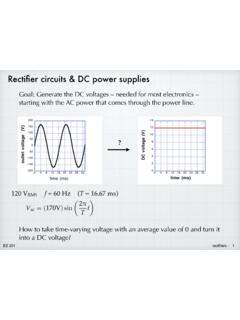
6 See specific models noted on pages 1 & 2 ENVIRONMENTAL parameterconditions/descriptionmintypmax unitsoperating temperaturesee derating curve-40105 Cstorage temperature-55125 Cstorage humiditynon-condensing95%temperature riseat full load, Ta=25 C25 CSOLDERABILITY parameterconditions/descriptionmintypmax unitshand mm from case for 10 seconds300 Creflow solderingsee reflow soldering profile245 CAdditional Resources: Product Page | 3D Model | PCB Inc SERIES: PDS1-M DESCRIPTION: DC-DC CONVERTER date 10/27/2022 page 4 of 8 PIN CONNECTIONSPINF unction1 GND2 Vin40V5+Vo8 NCunits: mm[inch]tolerance: [ ]pin section tolerance: [ ] MECHANICAL parameterconditions/descriptionmintypmax unitsdimensionssingle output models: x x output models: x x materialepoxy resin (UL94-V0)weightsingle output modelsdual output DRAWINGSINGLE OUTPUT MODELSA dditional Resources: Product Page | 3D Model | PCB Inc SERIES: PDS1-M DESCRIPTION.
7 DC-DC CONVERTER date 10/27/2022 page 5 of 8 PIN CONNECTIONSPINF unction1 GND2 Vin40V5-Vo7+Vo10 NCunits: mm[inch]tolerance: [ ]pin section tolerance: [ ] MECHANICAL DRAWING (CONTINUED)DUAL OUTPUT MODELSA dditional Resources: Product Page | 3D Model | PCB Inc SERIES: PDS1-M DESCRIPTION: DC-DC CONVERTER date 10/27/2022 page 6 of 8 EMC RECOMMENDED CIRCUITR ecommended external circuit componentsVout(dc) H10 H10 H1 F- F- F- H1 F- H1 F1nF/2kV F1nF/2kVFigure 1 Table 1 Single OutputsDual OutputsDERATING CURVESNote: 1.
8 See Cout values in Tables 1 and 2. 2. 24 Vdc output models require CY Resources: Product Page | 3D Model | PCB Inc SERIES: PDS1-M DESCRIPTION: DC-DC CONVERTER date 10/27/2022 page 7 of 81. Output load requirement To ensure this module can operate efficiently and reliably, the minimum output load may not be less than 10% of the full load during operation. If the actual output power is low, connect a resistor at the output end in parallel to increase the load. 2. Overload Protection Under normal operating conditions, the output circuit of this product has no protection against overload.
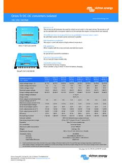
9 The simplest method to add this is to add a circuit breaker to the circuit. 3. Recommended circuit If you want to further decrease the input /output ripple, you can increase the capacitance accordingly or choose capacitors with low ESR (see Figure 2 & Table 1). However, the capacitance of the output filter capacitor must be appropriate. If the capacitance is too high, a startup problem might arise. For every channel of the output, to ensure safe and reliable operation, the maximum capacitance must be less than the maximum capacitive load (see Table 2).
10 It s not recommended to connect any external capacitors in applica-tions with less than watt NOTESNote: 1. Operation under minimum load will not damage the CONVERTER ; however, they may not meet all specifications listed. 2. Max. capacitive load tested at input voltage range and full load. 3. It is recommended to use either ceramic capacitors or electrolytic capacitors on the input and the output. Using tantalum capacitors may increase the risk of failure. 4. All specifications measured at: Ta=25 C, humidity<75%, nominal input voltage and rated output load, unless otherwise 2 Figure 3 Single Vout(Vdc)Max.