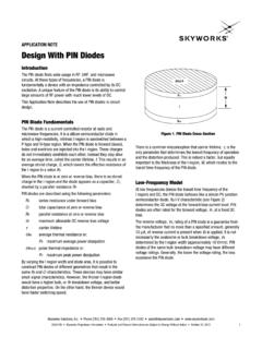
Transcription of Si510/511 Crystal Oscillator (XO) 100 kHz to 250 MHz
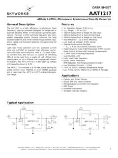
1 Skyworks Solutions, Inc. Phone [781] 376-3000 Fax [781] 376-3100 Skyworks Proprietary Information Products and Product Information are Subject to Change Without Notice October 29, 2021Si510/511 Crystal Oscillator (XO) 100 kHZ TO 250 MHZF eaturesApplicationsDescriptionThe Si510/511 XO utilizes Skyworks Solutions' advanced DSPLL technologyto provide any frequency from 100 kHz to 250 MHz. Unlike a traditional XOwhere a different Crystal is required for each output frequency, the Si510/511uses one fixed Crystal and Skyworks Solutions proprietary DSPLL synthesizer to generate any frequency across this range. This IC-basedapproach allows the Crystal resonator to provide enhanced reliability,improved mechanical robustness, and excellent stability. In addition, thissolution provides superior supply noise rejection, simplifying low jitter clockgeneration in noisy environments.
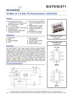
2 Crystal ESR and DLD are individuallyproduction-tested to guarantee performance and enhance reliability. TheSi510/511 is factory-configurable for a wide variety of user specifications,including frequency, supply voltage, output format, output enable polarity,and stability. Specific configurations are factory-programmed at time ofshipment, eliminating long lead times and non-recurring engineering chargesassociated with custom frequency Block Diagram Supports any frequency from 100 kHz to 250 MHz Low jitter operation 2 to 4 week lead times Total stability includes 10-year aging Comprehensive production test coverage includes Crystal ESR and DLD On-chip LDO regulator for power supply noise filtering , , or V operation Differential (LVPECL, LVDS, HCSL) or cmos output options Optional integrated 1:2 cmos fanout buffer Runt suppression on OE and power on Industry standard 5 x 7, x 5, and x mm packages Pb-free, RoHS compliant 40 to 85oC operation SONET/SDH/OTN Gigabit Ethernet Fibre Channel/SAS/SATA PCI Express 3G-SDI/HD-SDI/SDI Te l e c o m Switches/routers FPGA/ASIC clock generationVDDAny-Frequency to 250 MHz DSPLL SynthesisFixed Frequency OscillatorCLK+CLK OEGNDLow Noise RegulatorOrdering Information:See page Assignments:See page and +CLK NC123654 GNDNCVDDCLK+CLK OESi510(LVDS/LVPECL/HCSL/Dual cmos )Si510 ( cmos )Si511(LVDS/LVPECL/HCSL/Dual cmos )1243 GNDVDDCLKOE123654 GNDNCVDDCLK+CLK OESi510/5112 Skyworks Solutions, Inc.
3 Phone [781] 376-3000 Fax [781] 376-3100 Skyworks Proprietary Information Products and Product Information are Subject to Change Without Notice October 29, 2021 TABLE OF CONTENTSS ectionPage1. Electrical Specifications .. 32. Solder Reflow and Rework Requirements for mm Packages .. 113. Pin Descriptions .. Dual cmos Buffer .. 134. Ordering Information ..145. Si510/511 Mark Specification .. 156. Package Outline Diagram: 5 x 7 mm, 4-pin .. 167. PCB Land Pattern: 5 x 7 mm, 4-pin .. 178. Package Outline Diagram: 5 x 7 mm, 6-pin .. 189. PCB Land Pattern: 5 x 7 mm, 6-pin .. 1910. Package Outline Diagram: x 5 mm, 4-pin .. 2011. PCB Land Pattern: , 4-pin .. 2112. Package Outline Diagram: x 5 mm, 6-Pin .. 2213. PCB Land Pattern: x mm, 6-pin .. 2314. Package Outline Diagram: x mm, 4-pin .. 2415. PCB Land Pattern: x mm, 4-pin .. 2616. Package Outline Diagram: x mm, 6-pin.
4 2717. PCB Land Pattern: x mm, 6-pin .. 29 Revision History .. 30 Contact Information .. 31Si510/511 Skyworks Solutions, Inc. Phone [781] 376-3000 Fax [781] 376-3100 Skyworks Proprietary Information Products and Product Information are Subject to Change Without Notice October 29, 20211. Electrical SpecificationsTable 1. Operating SpecificationsVDD = V 5%, or V 10%, TA = 40 to +85oCParameterSymbolTest ConditionMinTypMaxUnitSupply V V V CurrentIDDCMOS, 100 MHz, single-ended 21 26mALVDS(output enabled) 19 23mALVPECL(output enabled) 39 43mAHCSL(output enabled) 41 44mATristate(output disabled) 18mAOE "1" SettingVIHSee x VDD VOE "0" SettingVILSee Note x VDDVOE Internal Pull-Up/Pull-Down Resistor*RI 45 k Operating TemperatureTA 40 85oC*Note: Active high and active low polarity OE options available. Active high option includes an internal pull-up.
5 Active low option includes an internal pull-down. See ordering information on page Solutions, Inc. Phone [781] 376-3000 Fax [781] 376-3100 Skyworks Proprietary Information Products and Product Information are Subject to Change Without Notice October 29, 2021 Table 2. Output Clock Frequency CharacteristicsVDD = V 5%, or V 10%, TA = 40 to +85oCParameterSymbolTest ConditionMinTypMaxUnitNominal FrequencyFOCMOS, Dual 250 MHzTotal Stability*Frequency Stability Grade C 30 +30ppmFrequency Stability Grade B 50 +50ppmFrequency Stability Grade A 100 +100ppmTemperature StabilityFrequency Stability Grade C 20 +20ppmFrequency Stability Grade B 25 +25ppmFrequency Stability Grade A 50 +50ppmStartup TimeTSUM inimum VDD until output frequency (FO) within specification 10msDisable TimeTDFO 10 MHz 5 sFO<10 MHz 40 sEnable TimeTEFO 10 MHz 20 sFO<10 MHz 60 s*Note: Total stability includes initial accuracy, operating temperature, supply voltage change, load change, shock and vibration (not under operation), and 10 years aging at Solutions, Inc.
6 Phone [781] 376-3000 Fax [781] 376-3100 Skyworks Proprietary Information Products and Product Information are Subject to Change Without Notice October 29, 2021 Table 3. Output Clock Levels and SymmetryVDD = V 5%, or V 10%, TA = 40 to +85oCParameterSymbolTest ConditionMinTypMaxUnitCMOS Output Logic x VDD VCMOS Output Logic LowVOL x VDDVCMOS Output Logic High V 8 V 6 V 4 mACMOS Output Logic Low V8 V6 V4 mACMOS Output Rise/Fall Time(20 to 80% VDD) to MHz,CL = 15 to MHz,CL = no Output Rise/Fall Time(20 to 80% VDD)TR/TF100 565psHCSL Output Rise/Fall Time (20 to 80% VDD)TR/TF100 470psLVDS Output Rise/Fall Time (20 to 80% VDD)TR/TF350 800psLVPECL Output Common ModeVOC50 to VDD 2 V, single-ended VDD V VLVPECL Output SwingVO50 to VDD 2 V, Output Common ModeVOC100 line-lineVDD= line-line, VDD= Output SwingVOSingle-ended, 100 differential Output Common ModeVOC50 to Output CycleDCAll formats485052%Si510/5116 Skyworks Solutions, Inc.
7 Phone [781] 376-3000 Fax [781] 376-3100 Skyworks Proprietary Information Products and Product Information are Subject to Change Without Notice October 29, 2021 Table 4. Output Clock Jitter and Phase Noise (LVPECL)VDD = or V 10%, TA = 40 to +85oC; Output Format = LVPECLP arameterSymbolTest ConditionMin TypMaxUnit Period Jitter (RMS)JPRMS10k samples1 Jitter(Pk-Pk)JPPKPK10k samples1 11ps Phase Jitter (RMS) MHz to 20 MHz integration bandwidth2 (brickwall) ps12 kHz to 20 MHz integration band-width2 (brickwall) Phase Noise, MHz N100Hz 86 dBc/Hz1 kHz 109 dBc/Hz10 kHz 116 dBc/Hz100 kHz 123 dBc/Hz1 MHz 136 dBc/HzAdditive RMS Jitter Due to External Power Supply Noise3 JPSR10 kHz sinusoidal noise ps100 kHz sinusoidal noise ps500 kHz sinusoidal noise ps1 MHz sinusoidal noise psSpuriousSPRLVPECL output, MHz, offset>10 kHz 75 to output frequencies: , , 75, , 100, , 125, , , 150, , , , 250 Applies to output frequencies: 100, , 125, , , 150, , , and 250 MHz.
8 Increase in jitter on output clock due to sinewave noise added to VDD ( V = 100 mVPP). Si510/511 Skyworks Solutions, Inc. Phone [781] 376-3000 Fax [781] 376-3100 Skyworks Proprietary Information Products and Product Information are Subject to Change Without Notice October 29, 2021 Table 5. Output Clock Jitter and Phase Noise (LVDS)VDD = V 5%, or V 10%, TA = 40 to +85oC; Output Format = LVDSP arameterSymbolTest ConditionMin TypMaxUnit Period Jitter (RMS)JPRMS10k samples1 Jitter(Pk-Pk)JPPKPK10k samples1 18ps Phase Jitter (RMS) MHz to 20 MHz integration bandwidth2 (brickwall) kHz to 20 MHz integration band-width2 (brickwall) Phase Noise, MHz N100Hz 86 dBc/Hz1 kHz 109 dBc/Hz10 kHz 116 dBc/Hz100 kHz 123 dBc/Hz1 MHz 136 dBc/HzSpuriousSPRLVPECL output, MHz, offset>10 kHz 75 to output frequencies: , , 75, , 100, , 125, , , 150, , , , 250 Applies to output frequencies: 100, , 125, , , 150, , , and 250 Solutions, Inc.
9 Phone [781] 376-3000 Fax [781] 376-3100 Skyworks Proprietary Information Products and Product Information are Subject to Change Without Notice October 29, 2021 Table 6. Output Clock Jitter and Phase Noise (HCSL)VDD = V 5%, or V 10%, TA = 40 to +85oC; Output Format = HCSLP arameterSymbolTest ConditionMin TypMaxUnit Period Jitter (RMS)JPRMS10k samples* Jitter(Pk-Pk)JPPKPK10k samples* 11ps Phase Jitter (RMS) MHz to 20 MHz integration bandwidth*(brickwall) kHz to 20 MHz integration band-width* (brickwall) Phase Noise, MHz N100Hz 90 dBc/Hz1kHz 112 dBc/Hz10 kHz 120 dBc/Hz100 kHz 127 dBc/Hz1 MHz 140 dBc/HzSpuriousSPRLVPECL output, MHz, offset>10 kHz 75 dBc*Note: Applies to an output frequency of 100 Solutions, Inc. Phone [781] 376-3000 Fax [781] 376-3100 Skyworks Proprietary Information Products and Product Information are Subject to Change Without Notice October 29, 2021 Table 7.
10 Output Clock Jitter and Phase Noise ( cmos , Dual cmos (Complementary))VDD = V 5%, or V 10%, TA = 40 to +85oC; Output Format = cmos , Dual cmos (Complementary)ParameterSymbolTest ConditionMin TypMaxUnitPhase Jitter (RMS) MHz to 20 MHz integration bandwidth2 (brickwall) kHz to 20 MHz integration band-width2 (brickwall) Phase Noise, MHz N100Hz 86 dBc/Hz1 kHz 108 dBc/Hz10 kHz 115 dBc/Hz100 kHz 123 dBc/Hz1 MHz 136 dBc/HzSpuriousSPRLVPECL output, MHz, offset>10 kHz 75 to output frequencies: , , 75, , 100, , 125, , , 150, , , Applies to output frequencies: 100, , 125, , , 150, , , 8. Environmental Compliance and Package InformationParameterConditions/Test MethodMechanical ShockMIL-STD-883, Method 2002 Mechanical VibrationMIL-STD-883, Method 2007 SolderabilityMIL-STD-883, Method 2003 Gross and Fine LeakMIL-STD-883, Method 1014 Resistance to Solder HeatMIL-STD-883, Method 2036 Contact PadsGold over NickelSi510/51110 Skyworks Solutions, Inc.