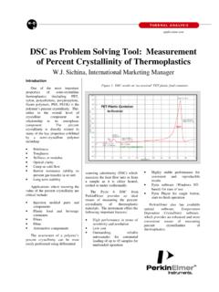
Transcription of Simple Method of Measuring the Band Gap Energy Value
1 IntroductionThe measurement of the band gap of materials is important in the semiconductor, nanomaterial and solar industries. This note demonstrates how the band gap of a material can be determined from its UV absorption term band gap refers to the Energy difference between the top of the valence band to the bottom of the conduction band (See Figure 1); electrons are able to jump from one band to another. In order for an electron to jump from a valence band to a conduction band , it requires a specific minimum amount of Energy for the transition, the band gap ,2 A diagram illustrating the bandgap is shown in Figure the band gap is important in the semiconductor and nanomaterial industries.
2 The band gap Energy of insulators is large (> 4eV), but lower for semiconductors (< 3eV). The band gap properties of a semiconductor can be controlled by using different semiconductor alloys such as GaAlAs, InGaAs, and InAlAs. A table of materials and bandgaps is given in Reference Spectrometerapplication noteSimple Method of Measuring the band Gap Energy Value of TiO2 in the Powder Form using a UV/Vis/NIR SpectrometerFigure 1. Explanation of band Dharma PerkinElmer Technical CenterAniruddha Pisal Global Application LaboratoryPerkinElmer, Inc. Shelton, CT USA2An alternative strategy is to use layers of different materials coated onto the silicon base material. This is employed in the solar industry in the construction of photovoltaic (PV) solar cells.
3 The bandgap is important as it determines the portion of the solar spectrum a photovoltaic cell Much of the solar radiation reaching the Earth is comprised of wavelengths with energies greater than the band gap of silicon. These higher energies will be absorbed by the solar cell, but the difference in Energy is converted into heat rather than into usable electrical Energy . Consequently, unless the band gap is controlled, the efficiency of the solar cell will be poor. Using layers of different materials with different band gap properties is a proven way to maximize the efficiency of solar cells. In the semiconductor and nanomaterial industries, titanium dioxide (TiO2, commonly known as titania) is added as an ingredient to coatings.
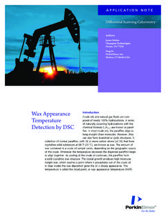
4 TiO2 is thought to promote the internal trapping of light by scattering (redirecting) the light reflected from the metallic electrode in the active layer and also to improve the transport of charge carriers through the active ExperimentalIt has been found that many of the nanomaterial studies on these materials are being carried out using a small quantity of the sample. Hence, sampling becomes a key issue to this type of analysis. The analysis was carried out using a LAMBDA 1050 UV/Vis/NIR spectrometer along with 150-mm integrating sphere (PerkinElmer, Inc., Shelton, CT USA) as shown in Figure 2. This holder (Prama Industries, Mumbai, India Figure 3) with powder sample in is clamped on the external port of the integrating sphere.
5 A low volume powder sample press was optical diagram of the integrating sphere is shown in Figure 2. LAMBDA 1050 UV/Vis/NIR System with Integrating 3. Powder sample press with sample 4. 150-mm Integrating Sphere Optical 5. UV WinLab Software sample was run using the parameters listed in Table 1. Instrumental range 250-800 nmSBW 2 nmData interval 1 nm The entrance port of the integrating sphere is kept open to minimize the specular reflection component which can cause fringes or noise at the extreme end of the range. The spectra were recorded in absorbance vs. wavelength and % reflectance vs. wavelength advantage of using a LAMBDA 1050 was to have a second sample compartment where the integrating sphere can be mounted without blocking the main sample compartment.
6 Results and DiscussionThe resulting spectrum obtained on TiO2 is shown in Figure spectral data recorded showed the strong cut off at nm; where the absorbance Value is minimum. The data is corroborated in the % Reflectance mode. CalculationsBand Gap Energy (E) = h*C/ (1 & 3)h = Planks constant = x 10-34 Joules secC = Speed of light = x 108 meter/sec = Cut off wavelength = x 10-9 meters H C E +08 1eV = X 10-19 Joules (conversion factor)Figure 6. TiO2 UV/Vis spectrum obtained in this 7. UV/Vis Absorption measurements for TiO2-(X) ZnFe2O4 nanocomposites. where X = Different molar concentration of ZnFe2O4. X = (dark green), (light green), (chocolate), (pink), (orange).
7 TiO2 Hydrolysis (blue), Pure TiO2 (violet).For a complete listing of our global offices, visit 2009-2102, PerkinElmer, Inc. All rights reserved. PerkinElmer is a registered trademark of PerkinElmer, Inc. All other trademarks are the property of their respective owners. 008684A_01 PerkinElmer, Inc. 940 Winter Street Waltham, MA 02451 USA P: (800) 762-4000 or (+1) similar experimental conditions and accessories, band gap Energy values for various powder nanomaterials can be calculated. With this, the quality of TiO2 also can be determined. Various other semiconductor nanomaterials can also be subjected to the experiment for which the example spectra from literature are given in Figure major advantages of using the specially designed small powder sample holder are: 1.
8 Smaller quantity powder samples can be analyzed directly 2. Due to a specially designed hand press, powder gets caked in the cup firmly and does not slip in to the sphere 3. Sample quantity required is 20-30 times less than the conventional powder sample holder 4. The press gives a very even surface to the sample to conduct reflectance experiments 5. Minimizes the specular component of the reflection as the sample is being exposed directly to the beam. 6. Cost effective sampling device with a depth of cm deep and 1 cm Hoffman, M., Martin, S., Choi, W., & Bahnemann, D. (1995). Environmental applications of semiconductor photo catalysis, Chemical Review, vol. 95, pp. Wikipedia: Bandgap definition and diagram, An Investigation of TiO2-ZnFe2O4 Nanocomposites for Visible Light Photo catalysis by Jeremy Wade, A thesis submitted to Department of Electrical Engineering; College of Engineering, University of South Florida, March 24, Fundamentals of Molecular Spectroscopy; Banwell University of Sussex, 3rd edition, May Wikipedia: Effect of TiO2 Nanoparticles on Polymer-Based Bulk Heterojunction Solar Cells ,Bandgap