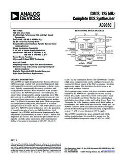
Transcription of Single and Dual, Ultralow Distortion, Ultralow …
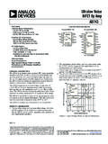
1 Single and dual , Ultralow distortion , Ultralow noise Op AmpsData Sheet AD8597/AD8599 Rev. F Document Feedback Information furnished by analog devices is believed to be accurate and reliable. However, no responsibility is assumed by analog devices for its use, nor for any infringements of patents or other rights of third parties that may result from its use. Specifications subject to change without notice. No license is granted by implication or otherwise under any patent or patent rights of analog devices . Trademarks and registered trademarks are the property of their respective owners. One Technology Way, Box 9106, Norwood, MA 02062-9106, : 2007 2017 analog devices , Inc. All rights reserved. Technical Support FEATURES Low noise : nV/ Hz at 1 kHz Low distortion : 120 dB THD at 1 kHz Input noise , Hz to 10 Hz: <76 nV p-p Slew rate: 14 V/ s Wide bandwidth: 10 MHz Supply current: mA/amp typical Low offset voltage: 10 V typical CMRR: 120 dB Unity-gain stable 15 V operation APPLICATIONS Professional audio preamplifiers ATE/precision testers Imaging systems Medical/physiological measurements Precision detectors/instruments Precision data conversion PIN CONFIGURATIONS 06274-060NC1 IN2+IN3V 4NC8V+7 OUT6NC5NC = NO CONNECTAD8597 TOP VIEW(Not to Scale) Figure 1.
2 AD8597 8-Lead SOIC (R-8) NC IN+INV V+NCOUTNC06274-061 NOTES1. NC = NO IT IS RECOMMENDED THAT THE EXPOSED PAD BE CONNECTED TO V .34126587AD8597 TOP VIEW(Not to Scale) Figure 2. AD8597 8-Lead LFCSP (CP-8-13) OUT A1 IN A2+IN A3 V4+V8 OUT B7 IN B6+IN B5AD8599 TOP VIEW(Not to Scale)06274-054 Figure 3. AD8599 8-Lead SOIC (R-8) GENERAL DESCRIPTION The AD8597/AD8599 are very low noise , low distortion opera-tional amplifiers ideal for use as preamplifiers. The low noise of nV/ Hz and low harmonic distortion of 120 dB (or better) at audio bandwidths give the AD8597/AD8599 the wide dynamic range necessary for preamplifiers in audio, medical, and instru-mentation applications. The excellent slew rate of 14 V/ s and 10 MHz gain bandwidth make them highly suitable for medical applications. The low distortion and fast settling time make them ideal for buffering of high resolution data converters.
3 The AD8597 is available in 8-lead SOIC and LFCSP packages, while the AD8599 is available in an 8-lead SOIC package. They are both specified over a 40 C to +125 C temperature range. The AD8597 and AD8599 are members of a growing series of low noise op amps offered by analog devices , Inc. (see Table 1). Table 1. Low noise Op Amps Package nV nV nV nV nV Single AD797 AD8597 ADA4004-1 AD8675 AD8671 dual AD8599 ADA4004-2 AD8676 AD8672 Quad ADA4004-4 AD8674 AD8597/AD8599 Data Sheet Rev. F | Page 2 of 20 TABLE OF CONTENTS Features .. 1 Applications .. 1 Pin Configurations .. 1 General Description .. 1 Revision History .. 2 Specifications .. 3 Absolute Maximum Ratings .. 5 Thermal Resistance .. 5 Power Sequencing .. 5 ESD Typical Performance Characteristics.
4 6 Functional 15 Input Voltage Range .. 15 Output Phase Reversal .. 15 noise and Source Impedance Considerations .. 15 Outline Dimensions .. 17 Ordering Guide .. 17 REVISION HISTORY 9/2017 Rev. E to Rev. F Changed CP-8-2 to CP-8-13 .. Throughout Updated Outline Dimensions .. 17 Changes to Ordering Guide .. 17 10/2013 Rev. D to Rev. E Change to Figure 15 Caption .. 7 Changes to Figure 23 and Figure 26 .. 9 Changes to Figure 30 and Figure 33 .. 10 Changes to Figure 46 through Figure 50 .. 13 Changes to Figure 53 and Figure 54 .. 14 2/2013 Rev. C to Rev. D Changes to Figure 44 .. 12 Changes to Figure 46 and Figure 49 .. 13 12/2009 R e v. B to Rev. C Changes to Table 1 .. 1 10/2008 R e v. A to Rev. B Added AD8597 .. Universal Added LFCSP_VD .. Universal Added Table 1 .. 1 Changes to Specifications Section .. 3 Changes to Absolute Maximum Ratings Section .. 5 Changes to Typical Performance Characteristics Section.
5 6 Added Figure 12 and Figure 15 .. 7 Added Figure 18 and Figure 19 .. 8 Added Figure 30 and Figure 33 .. 10 Added Figure 34 to Figure 38 .. 11 Added Figure 42 and Figure 45 .. 12 Added Figure 52, Figure 55, Figure 57 .. 14 Added Functional Operation Section .. 15 Added Figure 58 .. 15 Updated Outline Dimensions .. 17 Changes to Ordering Guide .. 17 4/2007 Rev. 0 to Rev. A Updated Layout .. 5 Changes to Figure 45 Caption .. 12 Added Figure 48 .. 12 Changes to Figure 51 Caption .. 13 2/2007 Revision 0: Initial Version Data Sheet AD8597/AD8599 Rev. F | Page 3 of 20 SPECIFICATIONS VSY = 5 V, VCM = 0 V, VO = 0 V, TA = 25 C, unless otherwise specified. Table 2. Parameter Symbol Conditions Min Typ Max Unit INPUT CHARACTERISTICS Offset Voltage VOS 15 120 V 40 C TA +125 C 180 V Offset Voltage Drift VOS/ T 40 C TA +125 C V/ C Input Bias Current IB 40 210 nA 40 C TA +125 C 340 nA Input Offset Current IOS 65 250 nA 40 C TA +125 C 340 nA Input Voltage Range IVR + V Common-Mode Rejection Ratio CMRR V VCM + V 120 135 dB 40 C TA +125 C 105 dB Large Signal Voltage Gain AVO RL 600.
6 VO = 11 V to +11 V 105 110 dB 40 C TA +125 C 100 dB Input Capacitance Differential Capacitance CDIFF pF Common-Mode Capacitance CCM pF OUTPUT CHARACTERISTICS Output Voltage High VOH RL = 600 V 40 C TA +125 C V RL = 2 k V 40 C TA +125 C V Output Voltage Low VOL RL = 600 V 40 C TA +125 C V RL = 2 k V 40 C TA +125 C V Output Short-Circuit Current ISC 52 mA Closed-Loop Output Impedance ZOUT At 1 MHz, AV = 1 5 POWER SUPPLY Power Supply Rejection Ratio PSRR VSY = 18 V to V 120 140 dB 40 C TA +125 C 118 dB Supply Current per Amplifier ISY mA 40 C TA +125 C mA DYNAMIC PERFORMANCE Slew Rate SR AV = 1, RL = 2 k 14 V/ s AV = 1, RL = 2 k 14 V/ s Settling Time tS To , step = 10 V 2 s Gain Bandwidth Product GBP 10 MHz Phase Margin M 60 Degrees noise PERFORMANCE Peak-to-Peak noise en p-p Hz to 10 Hz 76 nV p-p Voltage noise Density en f = 1 kHz nV/ Hz f = 10 Hz nV/ Hz Correlated Current noise f = 1 kHz pA/ Hz f = 10 Hz pA/ Hz Uncorrelated Current noise f = 1 kHz pA/ Hz f = 10 Hz pA/ Hz Total Harmonic distortion + noise THD + N G = 1, RL 1 k , f = 1 kHz, VRMS = 1 V 120 dB Channel Separation CS f = 10 kHz 120 dB AD8597/AD8599 Data Sheet Rev.
7 F | Page 4 of 20 VS = 15 V, VCM = 0 V, VO = 0 V, TA = +25 C, unless otherwise specified. Table 3. Parameter Symbol Conditions Min Typ Max Unit INPUT CHARACTERISTICS Offset Voltage VOS 10 120 V 40 C TA +125 C 180 V Offset Voltage Drift VOS/ T 40 C TA +125 C V/ C Input Bias Current IB 25 200 nA 40 C TA +125 C 300 nA Input Offset Current IOS 50 200 nA 40 C TA +125 C 300 nA Input Voltage Range IVR + V Common-Mode Rejection Ratio CMRR V VCM + V 120 135 dB 40 C TA +125 C 115 dB Large Signal Voltage Gain AVO RL 600 , VO = 11 V to +11 V 110 116 dB 40 C TA +125 C 106 dB Input Capacitance Differential Capacitance CDIFF pF Common-Mode Capacitance CCM pF OUTPUT CHARACTERISTICS Output Voltage High VOH RL = 600 V 40 C TA +125 C V RL = 2 k V 40 C TA +125 C V Output Voltage Low VOL RL = 600 V 40 C TA +125 C V RL = 2 k V 40 C TA +125 C V Output Short-Circuit Current ISC 52 mA Closed-Loop Output Impedance ZOUT At 1 MHz, AV = 1 5 POWER SUPPLY Power Supply Rejection Ratio PSRR VSY = 18 V to V 120 140 dB 40 C TA +125 C 118 dB Supply Current per Amplifier ISY mA 40 C TA +125 C mA DYNAMIC PERFORMANCE Slew Rate SR AV = 1, RL = 2 k 16 V/ s AV = 1, RL = 2 k 15 V/ s Settling Time ts To.
8 Step = 10 V 2 s Gain Bandwidth Product GBP 10 MHz Phase Margin M 65 Degrees noise PERFORMANCE Peak-to-Peak noise en p-p Hz to 10 Hz 76 nV p-p Voltage noise Density en f = 1 kHz nV/ Hz f = 10 Hz nV/ Hz Correlated Current noise f = 1 kHz pA/ Hz f = 10 Hz pA/ Hz Uncorrelated Current noise f = 1 kHz pA/ Hz f = 10 Hz pA/ Hz Total Harmonic distortion + noise THD + N G = 1, RL 1 k , f = 1 kHz, VRMS = 3 V 120 dB Channel Separation CS f = 10 kHz 120 dB Data Sheet AD8597/AD8599 Rev. F | Page 5 of 20 ABSOLUTE MAXIMUM RATINGS Table 4. Parameter Rating Supply Voltage 18 V Input Voltage V VIN +V Differential Input Voltage1 1 V Output Short-Circuit to GND Indefinite Storage Temperature Range 65 C to +150 C Operating Temperature Range 40 C to +125 C Lead Temperature Range (Soldering 60 sec) 300 C Junction Temperature 150 C 1 If the differential input voltage exceeds 1 V, limit the current to 5 mA.
9 Stresses at or above those listed under Absolute Maximum Ratings may cause permanent damage to the product. This is a stress rating only; functional operation of the product at these or any other conditions above those indicated in the operational section of this specification is not implied. Operation beyond the maximum operating conditions for extended periods may affect product reliability. THERMAL RESISTANCE JA is specified with the device soldered on a circuit board with its exposed paddle soldered to a pad (if applicable) on a 4-layer JEDEC standard PCB with zero air flow. Table 5. Package Type JA JC Unit 8-Lead LFCSP (CP-8 -13) 78 20 C/W 8-Lead SOIC (R-8) (AD8597) 140 39 C/W 8-Lead SOIC (R-8) (AD8599) 120 36 C/W POWER SEQUENCING Apply the op amp supplies simultaneously. The op amp supplies must be stable before any input signals are applied. In any case, the input current must be limited to 5 mA.
10 ESD CAUTION AD8597/AD8599 Data Sheet Rev. F | Page 6 of 20 TYPICAL PERFORMANCE CHARACTERISTICS TA = 25 C, unless otherwise noted. 75 65 55 45 35 25 15 515 25 35 45 55 65 755706050403020100 NUMBER OF AMPLIFIERSVOS ( V)AD8599 MEAN = = = = = 5V06274-001 Figure 4. Input Offset Voltage Distribution OF AMPLIFIERSTCVOS ( V)AD8599 MEAN = = = = = 5V06274-004 Figure 5. TCVOS Distribution, 40 C TA +125 C OF AMPLIFIERSTCVOS ( V)AD8599 MEAN = = = = = 5V06274-006 Figure 6. TCVOS Distribution, 40 C TA +85 C 75 65 55 45 35 25 15 515 25 35 45 55 65 755706050403020100 NUMBER OF AMPLIFIERSVOS ( V)AD8599 MEAN = = = = = 15V06274-002 Figure 7. Input Offset Voltage Distribution OF AMPLIFIERSTCVOS ( V)1050AD8599 MEAN = = = = = 15V06274-007 Figure 8.
