Transcription of Single Supply, Rail-to-Rail Low Power, FET-Input Op Amp ...
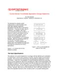
1 Single Supply, Rail-to-Rail Low Power, FET-Input Op Amp Data Sheet AD824 FEATURES Single supply operation: 3 V to 30 V Very low input bias current : 2 pA Wide input voltage range Rail-to-Rail output swing Low supply current per amplifier: 500 A Wide bandwidth: 2 MHz Slew rate: 2 V/ s No phase reversal APPLICATIONS Photo diode preamplifier Battery powered instrumentation Power supply control and protection Medical instrumentation Remote sensors Low voltage strain gage amplifiers DAC output amplifier PIN CONFIGURATION 1214135671098341211 OUT A IN A+IN AV++IN B IN BOUT BOUT D IN D+IN DV +IN C IN COUT CAD824 TOP VIEW(Not to Scale)00875-001 Figure 1. 14-Lead SOIC (R Suffix) GENERAL DESCRIPTION The AD824 is a quad, FET input , Single supply amplifier, featuring rail-to -rail outputs.
2 The combination of FET inputs and Rail-to-Rail outputs makes the AD824 useful in a wide variety of low voltage applications where low input current is a primary consideration. The AD824 is guaranteed to operate from a 3 V Single supply up to 15 V dual supplies. AD824AR-3V parametric performance at 3 V is fully guaranteed. Fabricated on Analog Devices, Inc., complementary bipolar process, the AD824 has a unique input stage that allows the input voltage to safely extend beyond the negative supply and to the positive supply without any phase inversion or latch-up. The output voltage swings to within 15 mV of the supplies. Capacitive loads to 350 pF can be handled without oscillation.
3 The FET input combined with laser trimming provides an input that has extremely low bias currents with guaranteed offsets below 1 mV. This enables high accuracy designs even with high source impedances. Precision is combined with low noise, making the AD824 ideal for use in battery powered medical equipment. Applications for the AD824 include portable medical equipment, photo diode preamplifiers, and high impedance transducer amplifiers. The ability of the output to swing Rail-to-Rail enables designers to build multistage filters in Single supply systems and maintain high signal-to-noise ratios. The AD824 is specified over the extended industrial ( 40 C to +85 C) temperature range and is available in narrow 14-lead SOIC package.
4 Rev. E Document Feedback Information furnished by Analog Devices is believed to be accurate and reliable. However, no responsibility is assumed by Analog Devices for its use, nor for any infringements of patents or other rights of third parties that may result from its use. Specifications subject to change without notice. No license is granted by implication or otherwise under any patent or patent rights of Analog Devices. Trademarks and registered trademarks are the property of their respective owners. One Technology Way, Box 9106, Norwood, MA 02062-9106, Tel: 2015 Analog Devices, Inc. All rights reserved. Technical Support AD824 Data Sheet TABLE OF CONTENTS Features.
5 1 Applications .. 1 Pin Configuration .. 1 General Description .. 1 Revision History .. 2 Specifications .. 3 Electrical Specifications .. 3 Absolute Maximum Ratings .. 6 Thermal Resistance .. 6 ESD Caution .. 6 Typical Performance Characteristics .. 7 Theory of Operation .. 12 input Characteristics .. 12 Output 12 Applications Information .. 13 Single Supply Voltage-to-Frequency Converter .. 13 Single Supply Programmable Gain Instrumentation Amplifier .. 13 3 V, Single Supply Stereo Headphone Driver .. 14 Low Dropout Bipolar Bridge Driver .. 14 A V/5 V Precision Sample-and-Hold Amplifier .. 15 Outline Dimensions .. 16 Ordering Guide .. 16 REVISION HISTORY 4/15 Rev.
6 D to Rev. E Change to Figure 1 Caption .. 1 5/14 Rev. C to Rev. D Updated Format .. Universal Removed 16-Lead SOIC Package (Throughout) .. 1 Deleted Wafer Test Limits Section .. 5 Deleted AD824 SPICE Macro-model Section .. 15 Changes to Ordering Guide .. 16 2/03 Rev. B to Rev. C Deleted N Package .. Universal Edits to General Description .. 1 Edits to Absolute Maximum Ratings .. 5 Edits to Ordering Guide .. 5 Edits to Figure 4 .. 12 Edits to Figure 8 .. 13 Updated Outline Dimensions .. 16 1/02 Rev. A to Rev. B Edits to Electrical Specifications .. 2, 3 Edits to Absolute Maximum Ratings .. 5 Edits to Ordering Guide .. 5 Deleted Dice Characteristics .. 5 Rev. E | Page 2 of 16 Data Sheet AD824 SPECIFICATIONS ELECTRICAL SPECIFICATIONS At VS = V, VCM = 0 V, VOUT = V, TA = 25 C; unless otherwise noted.
7 Table 1. Parameter Symbol Test Conditions/Comments Min Typ Max Unit input CHARACTERISTICS Offset Voltage (AD824A) VOS mV TMIN to TMAX mV input Bias current IB 2 12 pA TMIN to TMAX 300 4000 pA input Offset current IOS 2 10 pA TMIN to TMAX 300 pA input Voltage Range + V Common-Mode Rejection Ratio CMRR VCM = 0 V to 2 V 66 80 dB VCM = 0 V to 3 V 60 74 dB TMIN to TMAX 60 dB input Impedance 1013|| ||pF Large Signal Voltage Gain AVO VO = V to V RL = 2 k 20 40 V/mV RL = 10 k 50 100 V/mV RL = 100 k 250 1000 V/mV TMIN to TMAX, RL = 100 k 180 400 V/mV Offset Voltage Drift VOS/ T 2 V/ C OUTPUT CHARACTERISTICS Output Voltage High VOH ISOURCE = 20 A V TMIN to TMAX V ISOURCE = mA V TMIN to TMAX V Output Voltage Low VOL ISINK = 20 A 15 25 mV TMIN to TMAX 20 30 mV ISINK = mA 120 150 mV TMIN to TMAX 140 200 mV Short Circuit Limit ISC Sink/source 12 mA TMIN to TMAX 10 mA Open-Loop Impedance ZOUT f = 1 MHz, AV = 1 100 POWER SUPPLY Power Supply Rejection Ratio PSRR VS = V to 12 V 70 80 dB TMIN to TMAX 66 dB Supply current /Amplifier ISY TMIN to TMAX 500 600 A DYNAMIC PERFORMANCE Slew Rate SR RL = 10 k.
8 AV = 1 2 V/ s Full-Power Bandwidth BWP 1% distortion, VO = 4 V p-p 150 kHz Settling Time tS VOUT = V to V, to s Gain Bandwidth Product GBP 2 MHz Phase Margin o No load 50 Degrees Channel Separation CS f = 1 kHz, RL = 2 k 123 dB NOISE PERFORMANCE Voltage Noise en p-p Hz to 10 Hz 2 V p-p Voltage Noise Density en f = 1 kHz 16 nV/ Hz current Noise Density in f = 1 kHz fA/ Hz Total Harmonic Distortion THD f = 10 kHz, RL = , AV = +1 % Rev. E | Page 3 of 16 AD824 Data Sheet At VS = V, VOUT = 0 V, TA = 25 C; unless otherwise noted. Table 2. Parameter Symbol Test Conditions/Comments Min Typ Max Unit input CHARACTERISTICS Offset Voltage (AD824A) VOS mV TMIN to TMAX mV input Bias current IB VCM = 0 V 4 35 pA TMIN to TMAX 500 4000 pA IB VCM = 10 V 25 pA input Offset current IOS 3 20 pA TMIN to TMAX 500 pA input Voltage Range 15 +13 V Common-Mode Rejection Ratio CMRR VCM = 15 V to 13 V 70 80 dB TMIN to TMAX 66 dB input Impedance 1013|| ||pF Large Signal Voltage Gain AVO VO = 10 V to +10 V.
9 RL = 2 k 12 50 V/mV RL = 10 k 50 200 V/mV RL = 100 k 300 2000 V/mV TMIN to TMAX, RL = 100 k 200 1000 V/mV Offset Voltage Drift VOS/ T 2 V/ C OUTPUT CHARACTERISTICS Output Voltage High VOH ISOURCE = 20 A V TMIN to TMAX V ISOURCE = mA V TMIN to TMAX V Output Voltage Low VOL ISINK = 20 A V TMIN to TMAX V ISINK = mA V TMIN to TMAX V Short Circuit Limit ISC Sink/source, TMIN to TMAX 8 20 mA Open-Loop Impedance ZOUT f = 1 MHz, AV = 1 100 POWER SUPPLY Power Supply Rejection Ratio PSRR VS = V to 15 V 70 80 dB TMIN to TMAX 68 dB Supply current /Amplifier ISY VO = 0 V 560 625 A TMIN to TMAX 675 A DYNAMIC PERFORMANCE Slew Rate SR RL = 10 k , AV = 1 2 V/ s Full-Power Bandwidth BWP 1% distortion, VO = 20 V p-p 33 kHz Settling Time tS VOUT = 0 V to 10 V, to 6 s Gain Bandwidth Product GBP 2 MHz Phase Margin o 50 Degrees Channel Separation CS f = 1 kHz.
10 RL = 2 k 123 dB NOISE PERFORMANCE Voltage Noise en p-p Hz to 10 Hz 2 V p-p Voltage Noise Density en f = 1 kHz 16 nV/ Hz current Noise Density in f = 1 kHz fA/ Hz Total Harmonic Distortion THD f =10 kHz, VO = 3 V rms, RL = 10 k % Rev. E | Page 4 of 16 Data Sheet AD824 At VS = V, VCM = 0 V, VOUT = V, TA = 25 C; unless otherwise noted. Table 3. Parameter Symbol Test Conditions/Comments Min Typ Max Unit input CHARACTERISTICS Offset Voltage (AD824A 3 V) VOS mV TMIN to TMAX mV input Bias current IB 2 12 pA TMIN to TMAX 250 4000 pA input Offset current IOS 2 10 pA TMIN to TMAX 250 pA input Voltage Range 0 1 V Common-Mode Rejection Ratio CMRR VCM = 0 V to 1 V 58 74 dB TMIN to TMAX 56 dB input Impedance 1013|| ||pF Large Signal Voltage Gain AVO VO = V to V.