Transcription of SN54/74LS151 8-INPUT MULTIPLEXER - UCLM
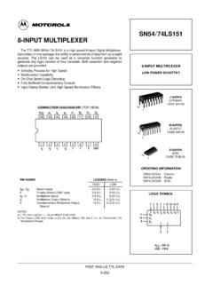
1 5-1 FAST AND LS TTL DATA8- input MULTIPLEXERThe TTL / MSI SN54 / 74LS151 is a high speed 8-INPUT Digital provides, in one package, the ability to select one bit of data from up to eightsources. The LS151 can be used as a universal function generator togenerate any logic function of four variables. Both assertion and negationoutputs are provided. Schottky Process for High Speed Multifunction Capability On-Chip Select Logic Decoding Fully Buffered Complementary Outputs input Clamp Diodes Limit High Speed Termination EffectsCONNECTION DIAGRAM DIP (TOP VIEW)14131211109123456716158 VCCI3I4I5I6I7S1S0S2I2I1I0 ZZEGNDPIN NAMESLOADING (Note a)HIGHLOWS0 S2EI0 I7 ZZSelect InputsEnable (Active LOW) InputMultiplexer InputsMultiplexer Output (Note b)Complementary MULTIPLEXER Output(Note b) ( ) ( ) :a) 1 TTL Unit Load ( ) = 40 A mA ) The Output LOW drive factor is for Military (54) and 5 for Commercial (74)Temperature MULTIPLEXERLOW POWER SCHOTTKYJ SUFFIXCERAMICCASE 620-09N SUFFIXPLASTICCASE 648-08161161 ORDERING INFORMATIONSN54 LSXXXJC eramicSN74 LSXXXN PlasticSN74 LSXXXD SOIC161D SUFFIXSOICCASE 751B-03 LOGIC SYMBOLVCC = PIN 16 GND = PIN 81110965743 2115141312EI0I1I2I3I4I5I6I7S0S1S2ZZ5-2 FAST AND LS TTL DATASN54/74LS151 LOGIC DIAGRAMS2S1S0EI0I1I2I3I4I5I6I7ZZ14126734 591112101315 VCC = PIN 16 GND = PIN 8 = PIN NUMBERSFUNCTIONAL DESCRIPTIONThe LS151 is a logical implementation of a single pole,8-position switch with the switch position controlled by thestate of three Select inputs, S0, S1, S2.
2 Both assertion andnegation outputs are provided. The Enable input (E) is activeLOW. When it is not activated, the negation output is HIGHand the assertion output is LOW regardless of all other logic function provided at the output is:Z = E (I0 S0 S1 S2 + I1 S0 S1 S2 + I2 S0 S1 S2+ I3 S0 S1 S2 + I4 S0 S1 S2 + I5 S0 S1 S2 + I6 S0 S1 S2 + I7 S0 S1 S2).The LS151 provides the ability, in one package, to selectfrom eight sources of data or control information. By propermanipulation of the inputs, the LS151 can provide any logicfunction of four variables and its TABLEES2S1S0I0I1I2I3I4I5I6I7 ZZHXXXXXXXXXXXHLLLLLLXXXXXXXHLLLLLHXXXXX XXLHLLLHXLXXXXXXHLLLLHXHXXXXXXLHLLHLXXLX XXXXHLLLHLXXHXXXXXLHLLHHXXXLXXXXHLLLHHXX XHXXXXLHLHLLXXXXLXXXHLLHLLXXXXHXXXLHLHLH XXXXXLXXHLLHLHXXXXXHXXLHLHHLXXXXXXLXHLLH HLXXXXXXHXLHLHHHXXXXXXXLHLLHHHXXXXXXXHLH H = HIGH Voltage LevelL = LOW Voltage LevelX = Don t Care5-3 FAST AND LS TTL DATASN54/74LS151 GUARANTEED OPERATING RANGESS ymbolParameterMinTypMaxUnitVCCS upply Ambient Temperature Range5474 550252512570 CIOHO utput Current High54, 74 Current CHARACTERISTICS OVER OPERATING TEMPERATURE RANGE (unless otherwise specified)
3 SblPLimitsUiTCdi iSymbolParameterMinTypMaxUnitTest ConditionsVIHI nput HIGH input HIGH Voltage forAll InputsVILI nput LOW input LOW Voltage forVILI nput LOW input LOW Voltage forAll InputsVIKI nput Clamp Diode Voltage = MIN, IIN = 18 mAVOHO utput HIGH = MIN, IOH = MAX, VIN = VIHVOHO utput HIGH MIN, IOH MAX, VIN VIHor VIL per Truth TableVOLO utput LOW Voltage54, = mAVCC = VCC MIN,VIN=VILor VIHVOLO utput LOW = mAVIN = VIL or VIHper Truth TableIIHI nput HIGH Current20 AVCC = MAX, VIN = VIIHI nput HIGH = MAX, VIN = VIILI nput LOW Current = MAX, VIN = VIOSS hort Circuit Current (Note 1) 20 100mAVCC = MAXICCP ower Supply Current10mAVCC = MAXNote 1: Not more than one output should be shorted at a time, nor for more than 1 CHARACTERISTICS (TA = 25 C)SblPLimitsUiTCdi iSymbolParameterMinTypMaxUnitTest ConditionstPLHtPHLP ropagation DelaySelect to Output Z27184330nsV50 VtPLHtPHLP ropagation DelaySelect to Output Z14202332nsV50 VtPLHtPHLP ropagation DelayEnable to Output Z26204232nsVCC = VtPLHtPHLP ropagation DelayEnable to Output Z15182430nsVCC VCL = 15 pFtPLHtPHLP ropagation DelayData to Output Z20163226nstPLHtPHLP ropagation DelayData to Output Z13122120nsAC WAVEFORMSF igure 1 Figure VtPLH