Transcription of SPECIFICATIONS CL(IDD) 9 cycle FEATURES
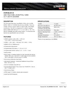
1 KVR13N9S8/44GB 1Rx8 512M x 64-Bit PC3-10600CL9 240-Pin DIMMDESCRIPTIONThis document describes ValueRAM's 512M x 64-bit (4GB)DDR3-1333 CL9 SDRAM (Synchronous DRAM), 1Rx8 memorymodule, based on eight 512M x 8-bit DDR3-1333 FBGA compo-nents. The SPD is programmed to JEDEC standard latencyDDR3-1333 timing of 9-9-9 at This 240-pin DIMM usesgold contact fingers. The electrical and mechanical specifica-tions are as follows: FEATURES JEDEC standard ( ~ ) Power Supply VDDQ = ( ~ ) 667 MHz fCK for 1333Mb/sec/pin 8 independent internal bank Programmable CAS Latency: 9, 8, 7, 6 Programmable Additive Latency: 0, CL - 2, or CL - 1 clock Programmable CAS Write Latency(CWL) = 7 (DDR3-1333) 8-bit pre-fetch Burst Length: 8 (Interleave without any limit, sequential withstarting address 000 only), 4 with tCCD = 4 which does notallow seamless read or write [either on the fly using A12 orMRS] Bi-directional Differential Data Strobe Internal(self) calibration: Internal self calibration through ZQpin (RZQ.)
2 240 ohm 1%) On Die Termination using ODT pin Average Refresh Period at lower than TCASE 85 C, at 85 C < TCASE < 95 C Asynchronous Reset PCB: Height ( ) or ( )Document No. 03/26/15 Page 1 Memory Module Specifi cations*Power will vary depending on the SDRAM 9)DDI(LCRow cycle Time (tRCmin) (min.)Refresh to Active/Refresh260ns (min.)Command Time (tRFCmin)Row Active Time (tRASmin)36ns (min.)Maximum Operating PowerTBD W*0 - V 49gnitaR LUOperating Temperature0o C to 85o CStorage Temperature-55o C to +100o CContinued >>Important Information: The module defined in this data sheet is one of several configurations available under this part number.
3 While all configurations are compatible, the DRAM combination and/or the module height may vary from what is described DIMENSIONS:Document No. Page 2