Transcription of The DIY Sony VFET - FIRST WATT
1 The DIY sony VFETby Nelson PassThis is an addendum to the sony SIT AMP part 2 article is the second of a series presenting Do-It- yourself audio power amplifiers using Static Induction Transistors (SITs), also known as vfets . These are unusual transistors with a characteristic similarity to Triode we are concerned with a modified version of the amplifier where we use only one pair of the VFET transistors per channel. The motivation for this is so that DIYers can build their own versions of the amplifier with the very limited quantities of the vfets which are make this design more accessible, is offering a limited number of kits for this design including vfets , pc boards, and refer you to previous articles (in pdf format) linked below. I recommend lookingat these for background sony VFET Part 22014 sony VFET Part 1 2013 sony VFET 40 Year Commemorative Amplifier 2011 SIT Introduction 2012 SIT Nemesis 2011 SIT-1 Owner's Manual 2011 SIT-2 Owner's Manual If you have absorbed the contents of the previous articles, you probably have a good picture of what is going on.
2 This project is simply a simplification of the Part 2 article, and virtually all you can see their will apply to this project, so you will want to pay particular attention to is the revised version of the circuit:Comparing it to Part 2, you see that there is only one pair of the vfets , that the input cascode transistors Q3 and Q4 are biased only by resistors, and that theregulators Q7 and Q8 are no longer bootstrapped by the output signal. Also, there is no longer a provision for no-feedback operation (we need the feedback here with the smaller output stage) and also no cascode still complex, it is a simpler circuit that Part 2, and more likely to be successfully built. Numerous resistor and transistor values have been adjusted, no big Notes:As with Part 2, I used an ordinary FIRST Watt type supply design, documented elsewhere, with 22 VAC transformer secondaries to provide +/-28 volts DC. 24 or 25 VAC will work fine, running a little hotter.
3 Later we will discuss changes to resistor values for different rail voltages. Also we will be giving more organized test procedures to maximize the probability of success in that scary moment when the power is FIRST article pretty much assumes that you are using the kit supplied by DIYA udio. The vfets provided with it are already tested and graded with a number which represents the bias voltage for amps of also offers a couple of chassis for this project, and the bracket which comes with the kit is designed to mount on one of their heat is nothing unusual regarding the construction of this amplifier. All the usual cautions and advice about building power amplifiers apply. There will be aconstruction thread and build video by 6L6 in the Pass Labs forum at Notes:The amplifier delivers 15 watts into 8 ohms and 20 watts into 4 ohms. This is less power that Part 2, and reflects the single pair of vfets .
4 The open loop gainis about 36 dB without a load, and 35 dB with an 8 ohm load, and the closed loop gain is 16 dB. The output impedance is ohms, a damping factor of are the curves:This is a curve showing the Class A envelope - current still going through the unused VFET at 15 watt rms (30 w peak) into 8 ohms. You can see that there is still about 100 mA bias left on the unused half of the amplifier at this reference, this is the artwork for the circuit board supplied in the kit. Green is the bottom traces, red is the top. Component numbers, polarities, and voltagetest points are silk screened in white on the top of the NOTESThe following notes are intended as an aid to initial testing and adjustment of this advanced do-it- yourself project. It is assumed that the builder has the skills and knowledge to safely tackle a project like this and is prepared to take responsibility for the 1 TESTING THE RESISTORSHere we will perform an early test to see if we have errors in resistor stuffing before we start putting in other parts.
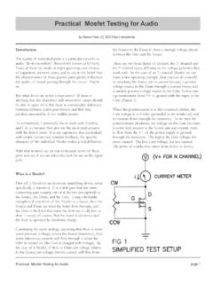
5 This will might just save us all sorts of trouble later resistors stuffed and soldered, no semiconductors or capacitors. All potentiometers set to halfway position. With digital ohmmeter, measure resistance between test points to about 5%. Don't get too excited if they aren't exact. Don't have an ohmmeter? Get T11680T8 T13680T2 T747T8 T947T6 T13250T10 T11250T6 T10430T8 T12430G IN49KG V+ 2 APPLYING POWER TO THE FRONT ENDC ircuit voltages with semis and capacitors stuffed NO vfets yet.** Pots P3 and P4 set fully counterclockwise **Power supply attached with V+ = +28V, V- = notes at end for other supply Voltages at test points:POINTSVOLTSPOINTSVOLTSG T6+28VG T8-28VG T4-24VG T2+24VT6 T70VT8 T90VT6 T11~ 5VT8 T13~ 5VG T18less than a few +/- volts (will adjust later)G T14+13VG T15-13VG T19~+12VG T20~-12VG T17~-10VG T16~+10 VPART 3 - BIASING UP THE FRONT ENDA ssuming you acquired them from DIYA udio, your vfets will have a Vgs rating written on them in tenths of volts (rating of 70 is Volts, and rating of 101 is Volts).
6 We want to set the voltages so the amplifiers comes up initially with low bias. The following voltages are reference to P1 for T16 equals the Vgs of 2SJ28 + 1V ( example: 68 wants + )Adjust P2 for T17 equals the Vgs of 2SK82 1V (example: 92 wants )Now we are going to bias up the front end Mosfets. We will be looking at the voltage drops across R5 (T6 and T7) and R6 (T8 and T9) as well as the DC offset at T18 (relative to ground) while adjusting the trim pots P3 and P4We are looking to achieve about volts across R5 and R6 and close to 0 voltsmeasured T18, which is the output of the front end your initial voltages across R5 and R6 with P3 and P4 counter-clockwise is above 1 volt, it is likely that either your Q1 and Q2 Jfets have particularly high Idss values and/or your Mosfets Q5 and Q6 have a low Vgs. If you encounter this, I suggest that you note the voltage drop between T6 and T11 and also between T8 and T13 and ask for help on the DIYA udio Pass Labs forum.
7 Do notcontinue to operate the circuit with R5 or R6 voltage drops above 2 start with P3 and P4 at counterclockwise positions which should be minimum bias, and ideally there will be no voltage across R5 and R6. If youhave voltage drops between 0 and 1 volt, you are still fine. If the initial voltage isabove 1 volt, skip to the end of Part are now going to adjust P3 and P4 with the following rotating procedure:Step 1 Check voltage across R5 (T6 to T7) and compare it to R6 (T8 to T9).If the voltage across R5 is less than and is lower than the voltage across R6, then adjust P3 clockwise to increase it by otherwise go to Step 2 Step 2 Check voltage across R6 (T8 to T9) and compare it to R5 (T6 to T7).If the voltage across R6 is less than and is lower than the voltage across R5, then adjust P4 clockwise to increase it by Repeat until the voltages across R5 and R6 are both at , matched as closely as you can get this point, the output voltage T18 should be fairly close to 0V.
8 By tweaking the values of R5 or R6 very gently, you should be able to get T18 to be fairly close to 0V while holding the resistor drops at about this point the circuit needs to warm up, and as it does the voltage across R5 and R6 (and thus the bias current of this stage) will rise a bit. If it climbs above , it will need to be adjusted downward, and the output offset re-adjusted. If it doesn't rise to , you can repeat the procedure to raise the value. Keep in mind that this is a good time to get these values and a low DC offset right. It becomes a little more complicated when the vfets are installed and the feedback loop starts readjust P1 and P2, as the adjustments of P3 and P4 will have slightly altered the voltages at T16 and it this way for a bit, and tweak the pots again for the desired voltages as outlined in this section, keeping in mind that each tweak will slightly alter the other values.
9 Halfway adjustments are still recommended. If it looks reasonably stable over a period of time, then we are ready for the final assembly and 4 INSTALLING vfets AND ADJUSTMENTAt this point, you install the vfets and prepare to fire up the previous instructions were intended to help you isolate and solve problems in the circuit prior to this step to minimize the chance that the rare and expensive vfets will not be damaged at this you have a Variac for this, you will want to use it, but keep in mind that it is only useful for providing a relatively low inrush current to the power supply capacitance you cannot raise the AC line voltage too slowly or you risk having the vfets draw too much current while the bias voltages are being suggest that you raise the AC line to voltage over a period of less than 5 's also a good idea to connect the channels up separately so that you are dealing with one at a time.
10 Until things are working, one channel at a time gets power supply V+ and also suggest that you start out with the lowest possible line fuse that can survive the modest inrush provided by the Variac. 1 amp fast blow is a goodstart, and has a reasonable chance of protecting the you don't have a Variac, you will probably need a higher value, but keep it at a minimum until you know the circuits are the 1 amp fuse survives, take a look at the voltages across R32 on each channel (test points -28V to T1) With a little luck it will be less than 100 it is higher, shut it down, adjust P1 and P2 counterclockwise a bit and try again. If that doesn't work, then stop and get , the R32 voltage drop will be about 50 mV or less, and you can move on to adjusting the output stage bias current and DC offset voltage. You do not need a load at the output for this procedure you will be adjusting P1 and P2 while keeping an eye on the voltage drop across the.