Transcription of Three-Dimensional Circuits LPKF LDS: Laser Direct ...
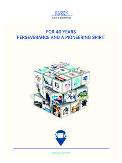
1 Three-Dimensional Circuits LPKF LDS: Laser Direct structuring for 3D Molded Interconnect Devices2 Innovative Product Design with MID TechnologyState-of-the-art technology: a circuit carrier was designed according to the LPKF LDS process for a complex dental tool. This makes a compact design and more functionality possible. The control for the warm water and air supply and a special lighting device are integrated in the hand Three-Dimensional circuit comes about without cables or separate circuit boards directly on the plastic carrier. The LPKF LDS process reduces the weight and diameter of the tool. That improves the ergonomics: Handling is pleasant and the manual stress on the hands is lowered. Contents 2 More Functionality New Possibilities 4 Flexible Solution for Three-Dimensional Circuits 6 Tomorrow s Technology in Today s Production 8 Inspiration for New Layouts 12 From the Idea to the LDS Prototype 14 The Advantages at a GlanceComponent for dental hand piece (Manufacturer: KaVo Dental GmbH)3 More Functionality New PossibilitiesSmartphone antenna structured with the LPKF Fusion3D 1100 Since 1997, LPKF has been working on Three-Dimensional circuit boards and has developed a Laser -supported process for producing Three-Dimensional MIDs (molded interconnect devices): the LPKF LDS process.
2 Circuit layouts can be created on complex Three-Dimensional carrier structures using LPKF Laser Direct Laser beam inscribes the layout directly on the plastic component. The weight and dimensions of the component can thus be noticeably reduced. Developers profit from complete 3-D capability on free-form surfaces and additional freedom in changing the circuit design. LPKF LDS opens up new Direct structuring takes place immediately after single-component injection molding of the carrier. A Laser beam requires only a few seconds to transfer the circuit layout directly from the computer to the plastic carrier without tools or masks. The subsequent metallization and SMD assembly lead to high-quality developed Solution for Three-Dimensional CircuitsA Better Product at a Lower CostTwo-component injection molding and hot stamping are recognized methods in producing MIDs (molded interconnect devices). Both processes are bound to product-specific tools in integrating conductor structures to a component.
3 Thus close-to-production prototyping is virtually impossible. The increasing miniaturization of Circuits on MID components is leading to a clear rise in the set-up time and the costs. The LPKF LDS process prevents these problems and increases cost-effectiveness in prototyping and series of the substantial advantages in processing materials with the Laser is the combination of a clearly defined energy input on the material and a high processing speed. The layout of the circuit is not predetermined by the geometry of a special tool. This makes a shorter development time and a higher degree of flexibility polymerLaserAdditive activated by Laser ablationLaser-structured and metallized finger tips for a robot hand(Source: Citec, Bielefeld University)5 The LPKF LDS Process1. Injection MoldingThe parts are produced in single-component injection molding from commercially available thermoplast provided with additives. In comparison to two-component injection molding, only one simple tool is required and the molding process is quicker.
4 You can find further information about the large LPKF portfolio of LDS-suitable materials on page Laser activationActivation of the thermoplastic material is done by Laser beam. A physical-chemical reaction creates metallic seeds that is the activation process. In addition to activation, the Laser forms a micro-rough surface on which the copper is firmly anchored during the MetallizationMetallization of the LPKF LDS parts begins with a cleaning step. After that, an additive track build-up takes place in copper baths, typically in a range of 8 to 12 m/h. Finally, as a rule a deposition of nickel and a thin layer of gold takes application-specific coatings such as Sn, Ag, Pd/Au, OSP, etc., can be applied in this AssemblyMany Laser -activatable plastics with a high level of heat resistance such as LCP, PA 6/6T or PBT/PET blend are reflow-solderable and thus compatible with standard SMT processes. When applying soldering paste, dispensing is the standard process if different height levels have to be achieved.
5 There are now several providers of technical solutions for Three-Dimensional pad on current -lessly metallized pad with Cu/Ni/AuSurface after Laser structuringSurface after metallizationStud bonds on metallized pad with Cu/Ni/Au6 Tomorrow s Technology in Today s ProductionThe increasing use of electronics is a challenge for many industries and markets. Industry requires technologies that reduce the dimensions and weight of components. At the same time, production of prototypes has to be simplified and the time until market launch has to be shortened. The LPKF LDS process meets these requirements LDS in Automotive EngineeringModern vehicles require a multitude of sensors and electronic assistants which increase the comfort and safety of the vehicle passengers. At the same time, the number of components used and the manufacturing costs should be clearly reduced. Injection-molded molded interconnect devices (MIDs) in combination with suitable connection and assembly technology are outstandingly suited for achieving these electro-mechanical functions such as keys, plugs and other connection elements can thus be integrated side by side in a component that serves as a molded interconnect in favor of LPKF LDS expands the design options, speeds up change of electronic components and leads to less expensive development and wheel controls(Manufacturer: TRW Automotive for BMW)7 Telecommunication Staying in ContactA multitude of types, design, miniaturization and cost reduction characterize the development of portable electronic devices.
6 End users expect more and more functions in up-to-date compact a New Generation of Medical DevicesSmaller dimensions, more functions these market requirements apply to many medical devices. New capabilities and technologies are pushing this trend: due to the rapid development in software and chip technology, new diagnostic procedures are constantly opening up. Small diagnostic devices help improve millions of patients lives. The patients can carry small diagnostic and monitoring devices for drug application, such as blood sugar measuring connection with widespread wireless communication technology, personal physician visits could be limited to a minimum. This development requires a new and higher stage of intelligent functional aggregation. The Laser -based LPKF LDS process exactly meets these requirements with its precision and high level of LPKF LDS technology has a large potential for miniaturization of components. At the same time, it offers a high level of flexibility when it s a matter of change and improvement of functionality especially if features are supposed to be variably adapted for several products.
7 Antennas in mobile phones and laptops produced with LPKF LDS technology have proven this millions of technology makes medical devices even more comfortable. A classic LPKF LDS application: hearing aids that are light and compact(Manufacturer: Siemens Audiologische Technik [Siemens Hearing Instruments])8 Pressure sensor for industrial applications. The ASIC is integrated; mechanical connections are part of the enclosure (Manufacturer: Harting AG)Combining flex circuit and plastic component into one component (Manufacturer: Harting AG)Inspiration for New LayoutsWhat is more convincing than projects that others have already successfully implemented? In the following, some applications represent the respective technical challenge. They illustrate how theoretical approaches have become real components and show the potential for LDS technology to develop in completely different Chip CarriersChanges to the circuit layout can be easily implemented by a change of the Laser program.
8 LPKF LDS technology thus opens up additional platform strategies for sensor enclosures. With suitable chip sets and circuit layouts, different products are developed on the basis of a common injection molded LPKF LDS process allows assembly with unhoused chips, e. g., through wire bonding or flip-chip technology. The process creates the smooth metal surfaces required for reliable Flex CircuitsIf the available installation space is limited, LPKF LDS prevents problems that occur with flex Circuits such as complex handling or limited bending electronics, medical technology, automobiles, telecommunication, consumer products LDS components are found in many devices and systems in many different areas of application and solve a whole range of demanding PlatingReliable through-hole plating can be produced with LPKF LDS technology in order to connect the surfaces of MIDs. This expands the possibilities for the layout. So applied, a 3D molded interconnect device serves to fix microphones in hearing aids according to the latest with SMTP roducts produced with LPKF LDS are completely SMT-capable.
9 Components on even surfaces of the same level can be mounted by automatic assembly. Meanwhile, serial systems are also available on the market for assembly of 3D and Ultra-Fine StructuresLPKF LDS implements extremely small track gaps. Track widths of 150 m (6 mil) and gaps of 200 m ( mil) have proven themselves as standard in practice. But also noticeably narrower tracks and gaps were already implemented in series produc-tion. The combination of small gaps and a compu-ter-controlled layout of complex Circuits expands the design possibilities of every for hearing aid (Manufacturer: Siemens Audiologische Technik GmbH [Siemens Hearing Instruments], Harting AG), images right: HSG-IMATD ental hand piece (Manufacturer: KaVo Dental GmbH) Top: safety enclosure (Manufacturer: Harting AG)Right: sensor structure on LCP Vectra E820i-LDS, lines and distances: 75 m / 75 m (3 mil / 3 mil) (Source: HSG-IMAT)200 mDiameter = 240 mLDS through-hole plating (Angle = 70 )1 mm200 m10 Steering wheel controls (Source: TRW Automotive for BMW)After a short chemical metallization, a smooth copper layer up to 35 m ( mil) thick comes about through classic galvanizationThe LDS enclosure connects the sensor and evaluation electronicsReliable ContactLDS components instead of wiring harnesses with LDS components additional cabling can be omitted.
10 Along with the costs of cabling, the assembly outlay is also reduced. If electronic components are soldered directly onto LDS components or attached by means of a conductive adhesive, additional circuit boards can often also be ReinforcementNew developments for new markets: with galvanic reinforcement, components come about that also withstand high mechanical and thermal stresses or are well suited to bonding due to their smooth metal TechnologyWith chip stacking, a LDS housing can take over the required contact between the components involved. A high packing density results with the slight pitch and the option of also using the outside of the housing or enclosure for on metallic bodies: a convincing answer to thermal problems in the LED areaClip N Slide LED light (Source: HomeLights/Molex)LED Clip SystemContact, attachment and heat conduction in one component. The functional components are arranged on a disk-shaped base medium. Two magnets hold the components, a metal layer on the bottom is for heat dissipation and LDS tracks supply the high-power LED with electric RetrofitTracks on metallic bodies?