Transcription of TNY284-290 TinySwitch-4 Family - Power Integrations
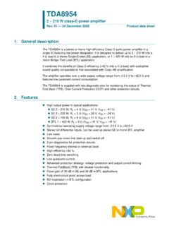
1 TNY284-290 . TinySwitch-4 Family Energy-Efficient, Off-Line Switcher with Line Compensated Overload Power Product Highlights + +. Lowest System Cost with Enhanced Flexibility DC. 725 V rated MOSFET Output Increases BV de-rating margin Line compensated overload Power no additional components Wide-Range Dramatically reduces max overload variation over universal input High-Voltage D. EN/UV. voltage range DC Input BP/M. 5% turn on UV threshold: line voltage sense with single external TinySwitch-4 . resistor S. Simple ON/OFF control, no loop compensation needed Selectable current limit through BP/M capacitor value PI-6578-020915. Higher current limit extends peak Power or, in open frame Figure 1. Typical Standby Application. applications, maximum continuous Power Lower current limit improves efficiency in enclosed adapters/. chargers Allows optimum tinyswitch -4 choice by swapping devices with no other circuit redesign Tight I2f parameter tolerance reduces system cost Maximizes MOSFET and magnetics utilization ON-time extension extends low-line regulation range/hold-up time SO-8C (D Package) DIP-8C (P Package) eSOP-12B (K Package).
2 To reduce input bulk capacitance Figure 2. Package Options. Self-biased: no bias winding or bias components Frequency jittering reduces EMI filter costs Pin-out simplifies heat sinking to the PCB Output Power Table SOURCE pins are electrically quiet for low EMI 230 VAC 15% 85-265 VAC. Enhanced Safety and Reliability Features Product3 Peak or Peak or Accurate hysteretic thermal shutdown protection with automatic Adapter1 Open Adapter1 Open recovery eliminates need for manual reset Frame2 Frame2. Auto-restart delivers <3% of maximum Power in short-circuit and TNY284P/D/K 6W 11 W 5W W. open loop fault conditions TNY285P/D W 15 W 6W W. Output overvoltage shutdown with optional Zener Fast AC reset with optional UV external resistor TNY285K 11 W 15 W W W. Very low component count enhances reliability and enables TNY286P/D 10 W 19 W 7W 15 W. single-sided printed circuit board layout TNY286K W 19 W W 15 W. High bandwidth provides fast turn-on with no overshoot and excellent transient load response TNY287P 13 W W 8W 18 W.
3 Extended creepage between DRAIN and all other pins improves field TNY287D W W 7W 18 W. reliability TNY287K 18 W W 11 W 18 W. EcoSmart Extremely Energy Efficient TNY288P 16 W 28 W 10 W W. Easily meets all global energy efficiency regulations No-load <30 mW with bias winding, <150 mW at 265 VAC without TNY288D W 26 W 9W W. bias winding TNY288K 23 W 28 W W W. ON/OFF control provides constant efficiency down to very light loads TNY289P 18 W 32 W 12 W 25 W. ideal for mandatory CEC regulations and EuP standby requirements TNY289K 25 W 32 W 17 W 25 W. Applications TNY290P 20 W W 14 W W. PC Standby and other auxiliary supplies DVD/PVR and other low Power set top decoders TNY290K 28 W W 20 W W. Supplies for appliances, industrial systems, metering, etc Table 1. Output Power Table. Chargers/adapters for cell/cordless phones, PDAs, digital cameras, Notes: MP3/portable audio, shavers, etc. 1. Minimum continuous Power in a typical non-ventilated enclosed adapter measured at +50 C ambient.
4 Use of an external heat sink will increase Power capability. 2. Minimum peak Power capability in any design or minimum continuous Power in an open frame design (see Key Applications Considerations). 3. Packages: P: DIP-8C, D: SO-8C, K: eSOP-12B. See Part Ordering Information. August 2016. This Product is Covered by Patents and/or Pending Patent Applications. TNY284-290 . BYPASS/. MULTI-FUNCTION DRAIN. (BP/M) (D). REGULATOR. V. LINE UNDERVOLTAGE. 25 A. FAULT BYPASS PIN. PRESENT UNDER-VOLTAGE. +. AUTO- BYPASS. 115 A RESTART - CAPACITOR. COUNTER SELECT AND V VI. CURRENT V LIMIT LINE. RESET LIMIT STATE COMPENSATION. MACHINE. CURRENT LIMIT. COMPARATOR. ENABLE - +. ENABLE/ V + VT JITTER. UNDER- CLOCK. VOLTAGE THERMAL. DCMAX. (EN/UV) SHUTDOWN. V OSCILLATOR. S Q. R Q. V LEADING. OVP EDGE. LATCH BLANKING. SOURCE. (S). PI-6639-072115. Figure 3. Functional Block Diagram. Pin Functional Description D Package (SO-8C). DRAIN (D) Pin: This pin is the Power MOSFET drain connection.
5 It provides internal EN/UV 1 8S. operating current for both start-up and steady-state operation. BP/M 2 7S. BYPASS/MULTI-FUNCTION (BP/M) Pin: This pin has multiple functions: 6S. It is the connection point for an external bypass capacitor for the D4 5S P Package (DIP-8C). internally generated V supply. It is a mode selector for the current limit value, depending on the EN/UV 1 8S. value of the capacitance added. Use of a F capacitor results BP/M 2 7S. in the standard current limit value. Use of a 1 F capacitor results Exposed Pad (On Bottom). in the current limit being reduced to that of the next smaller device Internally Connected to SOURCE Pin 6S. size. Use of a 10 F capacitor results in the current limit being K Package increased to that of the next larger device size for TNY285-290. (eSOP-12B) D4 5S. It provides a shutdown function. When the current into the bypass pin exceeds ISD, the device latches off until the BP/M voltage EN/UV 1 12 S.
6 Drops below V, during a Power -down or, when the UV function BP/M 2 11 S. is employed with external resistors connected to the BP/UV pin, by N/C 3 10 S. taking the UV/EN pin current below IUV minus the reset hysteresis (Typ. A). This can be used to provide an output overvolt- N/C 4 9S. age function with a Zener connected from the BYPASS/MULTI- 8S. FUNCTIONAL pin to a bias winding supply. D6 7S. PI-6577-021015. Figure 4. Pin Configuration. 2. Rev. D 08/16 TNY284-290 . ENABLE/UNDERVOLTAGE (EN/UV) Pin: The frequency jitter should be measured with the oscilloscope This pin has dual functions: enable input and line undervoltage sense. triggered at the falling edge of the DRAIN waveform. The waveform During normal operation, switching of the Power MOSFET is controlled in Figure 5 illustrates the frequency jitter. by this pin. MOSFET switching is terminated when a current greater Enable Input and Current Limit State Machine than a threshold current is drawn from this pin.
7 Switching resumes The enable input circuit at the ENABLE/UNDERVOLTAGE pin consists when the current being pulled from the pin drops to less than a of a low impedance source follower output set at V. The current threshold current. A modulation of the threshold current reduces through the source follower is limited to 115 A. When the current group pulsing. The threshold current is between 75 A and 115 A. out of this pin exceeds the threshold current, a low logic level (disable). The ENABLE/UNDERVOLTAGE pin also senses line undervoltage is generated at the output of the enable circuit, until the current out conditions through an external resistor connected to the DC line of this pin is reduced to less than the threshold current. This enable voltage. If there is no external resistor connected to this pin, circuit output is sampled at the beginning of each cycle on the rising TinySwitch-4 detects its absence and disables the line undervoltage edge of the clock signal.
8 If high, the Power MOSFET is turned on for function. that cycle (enabled). If low, the Power MOSFET remains off (disabled). Since the sampling is done only at the beginning of each cycle, SOURCE (S) Pin: subsequent changes in the ENABLE/UNDER- VOLTAGE pin voltage or This pin is internally connected to the output MOSFET source for current during the remainder of the cycle are ignored. high-voltage Power return and control circuit common. The current limit state machine reduces the current limit by discrete TinySwitch-4 Functional Description amounts at light loads when TinySwitch-4 is likely to switch in the TinySwitch-4 combines a high-voltage Power MOSFET switch with a audible frequency range. The lower current limit raises the effective Power supply controller in one device. Unlike conventional PWM (pulse switching frequency above the audio range and reduces the trans- width modulator) controllers, it uses a simple former flux density, including the associated audible noise.
9 The state ON/OFF control to regulate the output voltage. machine monitors the sequence of enable events to determine the load condition and adjusts the current limit level accordingly in The controller consists of an oscillator, enable circuit (sense and logic), discrete amounts. current limit state machine, V regulator, BYPASS/MULTI- FUNCTION pin undervoltage, overvoltage circuit, and current limit Under most operating conditions (except when close to no-load), the selection circuitry, over-temperature protection, current limit circuit, low impedance of the source follower keeps the voltage on the leading edge blanking, and a 725 V Power MOSFET. TinySwitch-4 ENABLE/UNDERVOLTAGE pin from going much below V in the incorporates additional circuitry for line undervoltage sense, disabled state. This improves the response time of the optocoupler auto-restart, adaptive switching cycle on-time extension, and that is usually connected to this pin. frequency jitter.
10 Figure 3 shows the functional block diagram with V Regulator and V Shunt Voltage Clamp the most important features. The V regulator charges the bypass capacitor connected to the Oscillator BYPASS pin to V by drawing a current from the voltage on the The typical oscillator frequency is internally set to an average of DRAIN pin whenever the MOSFET is off. The BYPASS/MULTI- 132 kHz. Two signals are generated from the oscillator: the maximum FUNCTION pin is the internal supply voltage node. When the duty cycle signal (DCMAX) and the clock signal that indicates the MOSFET is on, the device operates from the energy stored in the beginning of each cycle. bypass capacitor. Extremely low Power consumption of the internal circuitry allows TinySwitch-4 to operate continuously from current it The oscillator incorporates circuitry that introduces a small amount of takes from the DRAIN pin. A bypass capacitor value of F is frequency jitter, typically 8 kHz peak-to-peak, to minimize EMI sufficient for both high frequency decoupling and energy storage.