Transcription of Understanding DRAM Operation
1 Applications NoteUnderstanding DRAM Operation12/96 Page 1 OverviewDynamic random access memory (DRAM) devicesare used in a wide range of electronics they are produced in many sizes and soldin a variety of packages, their overall Operation isessentially the are designed for the sole purpose of storingdata. The only valid operations on a memory deviceare reading the data stored in the device, writing (orstoring) data in the device, and refreshing the dataperiodically. To improve efficiency and speed, anumber of methods for reading and writing the mem-ory have been document describes basic asynchronousDRAM Operation , including some of the most com-monly used features for improving DRAM perfor-mance. While many aspects of a synchronousDRAM are similar to an asynchronous DRAM, syn-chronous Operation differs because it uses a clockedinterface and multiple bank architecture. Additionalinformation regarding specific features and designissues may be found in the Applications ArchitectureDRAM chips are large, rectangular arrays of mem-ory cells with support logic that is used for readingand writing data in the arrays, and refresh circuitry tomaintain the integrity of stored ArraysMemory arrays are arranged in rows and columns ofmemory cells called wordlines and bitlines, respec-tively.
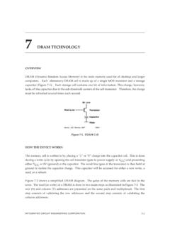
2 Each memory cell has a unique location oraddress defined by the intersection of a row and CellsA DRAM memory cell is a capacitor that is chargedto produce a 1 or a 0. Over the years, several differ-ent structures have been used to create the memorycells on a chip. In today's technologies, trenchesfilled with dielectric material are used to create thecapacitive storage element of the memory CircuitryThe memory chip's support circuitry allows the userto read the data stored in the memory 's cells, write tothe memory cells, and refresh memory cells. Thiscircuitry generally includes: Sense amplifiers to amplify the signal or chargedetected on a memory cell. Address logic to select rows and columns. Row Address Select (RAS) and ColumnAddress Select (CAS) logic to latch and resolvethe row and column addresses and to initiateand terminate read and write operations. Read and write circuitry to store information inthe memory 's cells or read that which is storedthere. Internal counters or registers to keep track of therefresh sequence, or to initiate refresh cycles asneeded.
3 Output Enable logic to prevent data fromappearing at the outputs unless 1: IBM Trench Capacitor MemoryCellP+P+Word LineStrapN-wellP- SubstrateBit LineNote: Not to ScaleTransfer NodeTrench CapacitorColumn AddressRow AddressApplications NoteUnderstanding DRAM OperationPage 212/96 Understanding the DRAM Timing DiagramThe most difficult aspect of working with DRAM devices is resolving the timing are generally asynchronous, responding toinput signals whenever they occur. As long as thesignals are applied in the proper sequence, with sig-nal durations and delays between signals that meetthe specified limits, the DRAM will work datasheets for our products contain timing dia-grams for the particular devices. You may want toview a relevant timing diagram while reading theinformation are only a few signals that control the opera-tion of a Address Select (Strobe) (RAS)TheRAS cir-cuitry is used to latch the row address and to initiatethe memory cycle. It is required at the beginning ofevery is active low; that is, to enableRAS, a transition from a high voltage to a low volt-age level is required.
4 The voltage must remain lowuntilRAS is no longer needed. During a completememory cycle, there is a minimum amount of timethatRAS must be active (tRAS), and a minimumamount of time thatRAS must be inactive, called theRAS precharge time (tRP).RAS may also be used totrigger a refresh cycle (RAS Only Refresh, or ROR).Column Address Select (Strobe) (CAS)CAS isused to latch the column address and to initiate theread or write may also be used totrigger aCAS beforeRAS refresh cycle. This refreshcycle requiresCAS to be active prior toRAS and toremain active for a specified time. It is active memory specification lists the minimum amountof timeCAS must remain active (tCAS) to initiate aread or write Operation . For most memory opera-tions, there is also a minimum amount of time thatCAS must be inactive, called theCAS prechargetime (tCP). (An ROR cycle does not requireCAS tobe active.)AddressThe addresses are used to select a mem-ory location on the chip. The address pins on amemory device are used for both row and columnaddress selection (multiplexing).
5 The number ofaddresses depends on the memory s size and orga-nization. The voltage level present at each addressat the time thatRAS orCAS goes active determinesthe row or column address, respectively, that isselected. To ensure that the row or column addressselected is the one that was intended, set up andhold times with respect to theRAS andCAS transi-tions to a low level are specified in the DRAM Enable (WE)The write enable signal is usedto choose a read Operation or a write Operation . Alow voltage level signifies that a write Operation isdesired; a high voltage level is used to choose aread Operation . The Operation to be performed isusually determined by the voltage level onWE whenCAS goes low (Delayed Write is an exception). Toensure that the correct Operation is selected, set upand hold times with respect toCAS are specified inthe DRAM timing Enable (OE)During a read Operation , thiscontrol signal is used to prevent data from appearingat the output until needed. WhenOE is low, dataappears at the data outputs as soon as it is is ignored during a write Operation .
6 In manyapplications, theOE pin is grounded and is not usedto control the DRAM In or Out (DQs)The DQ pins (also calledInput/Output pins or I/Os) on the memory device areused for input and output. During a write Operation , avoltage (high=1, low=0) is applied to the DQ. Thisvoltage is translated into the appropriate signal andstored in the selected memory cell. During a readoperation, data read from the selected memory cellappears at the DQ once access is complete and theoutput is enabled (OE low). At most other times, theDQs are in a high impedance state; they do notsource or sink any current, and do not present a sig-nal to the system. This also prevents DQ contentionwhen two or more devices share the data NoteUnderstanding DRAM Operation12/96 Page 3 Reading Data From MemoryFigure 2 is the timing diagram of a simplified Readcycle that illustrates the following read the data from a memory cell, the cell mustbe selected by its row and column coordinates, thecharge on the cell must be sensed, amplified, andsent to the support circuitry, and the data must besent to the data output.
7 In terms of timing, the follow-ing steps must occur:1. The row address must be applied to the addressinput pins on the memory device for the pre-scribed amount of time beforeRAS goes low(tASR) and held (tRAH) afterRAS goes must go from high to low and remain low(tRAS).3. A column address must be applied to theaddress input pins on the memory device for theprescribed amount of time (tASC) and held (tCAH)afterCAS goes must be set high for a read Operation tooccur prior (tRCS) to the transition ofCAS, andremain high (tRCH) after the transition must switch from high to low and remainlow (tCAS). goes low within the prescribed window oftime. CyclingOE is optional; it may be tied low, Data appears at the data output pins of thememory device. The time at which the dataappears depends on whenRAS (tRAC),CAS(tCAC), andOE (tOEA) went low, and when theaddress is supplied (tAA).8. Before the read cycle can be considered com-plete,CAS andRAS must return to their inactivestates (tCRP, tRP).
8 Figure 2. Simplified Read CycleRASVIHVILVIHVILA ddressVIHVILWEVIHVILOEVIHVILDOUTVOHVOLRo wColumnValid Data OuttRAStRPtRCtCAStRAHtASCtCAHtASRtRCStOF FtCACtRACHi-ZHi-ZtRCH: H or L tAAtOEACAS tCRPA pplications NoteUnderstanding DRAM OperationPage 412/96 Using Fast Page Mode and EDOA number of read options have been developed toimprove system performance when reading include Fast Page Mode (FPM), ExtendedData Out (EDO) Mode (formerly called Hyper PageMode or HPM), and burst data using SynchronousDRAMs. All three of these methods rely on the abil-ity to access all of the data stored in a page withouthaving to initiate a completely new memory DRAMs are described in the Applica-tions Note Synchronous DRAMs: The DRAM of theFuture. A page is defined as all of the memory cells thathave a common row address and are wired to a page is as many bits long as the number ofcolumn addresses being accessed, ranging from aminimum of two to a maximum of whatever numberof columns are in the device's memory array (forexample, IBM's 1Mx4 chip can have a page as longas 1024 bits.)
9 The number of full pages (all columnaddresses on a row) on a memory chip is equal tothe number of rows times the number of data DQs(or I/Os). The block diagrams in the datasheetsshow the number of rows, columns, and DQs (I/Os)for each DRAM Page Mode (FPM)To read data using Fast Page Mode, start as youwould a normal read Operation (steps 1 through 7 inthe Reading Data From memory sequence listedabove.) Once the data is valid, switchCAS andOEhigh, but leaveRAS low. WhenCAS has been inac-tive (high) for the required amount of time (tCP),repeat steps 3 through 7 of the read Operation . Youcan continue in this way until a new row address isrequired or the chip needs to be doesnot have to be cycled. If it remains low, the data out-puts will be disabled whenCAS goes 3 is a complete timing diagram that illustratesa Fast Page Mode read Data Out (EDO) or Hyper PageModeEDO is very similar to FPM. The main difference isthat the data output drivers are not disabled whenCAS goes high on the EDO DRAM, allowing thedata from the current read cycle to be present at theoutputs while the next read cycle begins, and result-ing in a faster cycle time.
10 Figure 4 is a complete tim-ing diagram that illustrates an EDO mode Applications Note "EDO (Hyper Page Mode)"explains Fast Page Mode and EDO Operation inmore NoteUnderstanding DRAM Operation12/96 Page 5 Figure 3. Fast Page Mode Read CycleRASVIHVILVIHVILVIHVILWEVIHVILOEVIHV ILVIHVILVOHVOLtRASP: H or L RowColumn 1 Column 2 Column nDOUT1 DOUT 2 DOUT NtASRtASCtRAHtCAHtCSHtASCtCAHtASCtCAHtCA StRSHtCAStCAStPCtCPtCRPtRADtRCHtRCStRCHt RCStRCHtRRHtAARCSttOEAtOEAtCPAtAAtOEAtCP AtCLZtOFFtOFFtOFFOEZttOEZtOEZtDZCtDZOtCA CtOEDtOEDtCDDtCLZtCACtCACtCPtOHtOHOtCPRH A ddressDINDOUTtRPtRCDtOHtOHOtOHtCALtRACtO HOtOEDtRALtDZCtDZCtDZOtDZOtCLZCAStAAAppl ications NoteUnderstanding DRAM OperationPage 612/96 Figure 4. EDO (Hyper Page) Mode Read CycletRPtHCASData Out 1 Data Out 2 OEWERASRowAddressColumn 1 Column 2 Column NtOEAtDOHtDOHtOEZtCLZtCACVIHVILtASRtRAHt ASCtASCtCAHtCAHtCAHDOUTtRASPtCPRHtCRPtRS HtHCAStHCAStHPCtASCtCSHtRADtRCStCACtCPAt CPAtAAtAAtRACtAAHi-Z: H or L tRALVIHVILVIHVILVIHVILVIHVILVOHVOLtRCDtC PtCPtRRHtRCHtWPtCACData Out NtOFFCAStWRPNOTE 1tWRHNOTE 1: ImplementingWE atRAS time during a Read or Write Cycle is so will facilitate compatibility with future EDO NoteUnderstanding DRAM Operation12/96 Page 7 Writing Data To MemoryFigure 3 is the timing diagram of a simplified Writecycle that illustrates described write to a memory cell, the row and columnaddress for the cell must be selected and data mustbe presented at the data input pins.