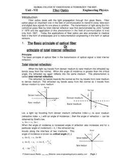
Transcription of Unit –IV Semiconductors Engineering Physics
1 unit IV Semiconductors Engineering Physics Dr. Reddy , PhD Website: Page 1 Introduction A semiconductor is a material that has a resistivity lies between that of a conductor and an insulator. The conductivity of a semiconductor material can be varied under an external electrical field. Devises made from semiconductor materials are the foundation of modern electronics, including computer, radio, telephones and many other devises. In a metallic conductor, current is carried by the flow of electrons. In Semiconductors , current can be carried by either flow of electrons or flow of holes or both. Germanium and Silicon are the best examples for semiconductor materials. Both are tetravalent ( four valence electrons) and both have diamond crystal structure. At T=0K, the semiconductor acts as insulator. Semiconductors are classified into two types, they are 1.
2 Intrinsic semiconductor 2. Extrinsic semiconductor 1. Intrinsic semiconductor A pure semiconductor is called intrinsic semiconductor. A pure crystal of Germanium and Silicon is an example for intrinsic semiconductor. At T=0K, the semiconductor acts as insulator. Germanium and silicon are tetravalent atoms ( four valence electrons) and both have diamond crystal structure. In order to gain stability each germanium atom makes four covalent bonds with the four surrounding germanium atoms by sharing of their valence electrons as shown in figure. At 0K, the semiconductor crystal acts as a perfect insulator since the covalent bonds are strong and no free electrons are available. At room temperature (T>0K) the semiconductor gives some conductivity since some of the covalent bonds are broken due to the thermal energy supplied to the crystals. The vacancy of an electron in the covalent is called hole.
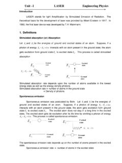
3 Thus the valence band has holes and conduction band has electrons For silicon energy gap is and for germanium energy gap is In intrinsic semiconductor the electron concentration is equal to the hole concentration. In intrinsic Semiconductors Fermi level is always lies between valence band and conduction band. 2 The law of mass action for intrinsic Semiconductors is In intrinsic semiconductor the carrier concentration of electrons (n) and holes (p) is unit IV Semiconductors Engineering Physics Dr. Reddy , PhD Website: Page 2 2. Intrinsic carrier concentration In intrinsic semiconductor pn= Hence inpn== is called intrinsic carrier concentration.. Where gVCEEE= is the forbidden gap. !/ The above equation shows the intrinsic carrier concentration. 3. Fermi level in intrinsic semiconductor In intrinsic semiconductor pn= kTEEEVCFe)(2(+ Taking logarithms on both sides CVNNlog kTEEEVCF)(2+ xexe=logQ CVNNKTlog )(2 VCFEEE+ FE2 )(VCEE+ CVNNKTlog unit IV Semiconductors Engineering Physics Dr.)
4 Reddy , PhD Website: Page 3 2)(log2 CVVcFEENNKTE++ = If we assume that CN=VN 2 VCFEEE+= Thus the Fermi level in intrinsic semiconductor is always lies between the valence band and conduction band. 4. Intrinsic conductivity In semiconductor, the electrons and holes will participate in electrical conductivity. To obtain an expression for electrical conductivity, we consider a rectangular bar of intrinsic semiconductor connected to a battery is shown in figure. When an electric field is applied along X-axis, the electrons move along negative X-axis and holes move along X-axis. Due to field, the charge carriers attain some constant velocity. This constant velocity is called drift velocity, represented by #$. #$ % (1) Let n be the concentration of electrons in semiconductor. Then the current density due to an electron is &' #$ (2) From equations (1) and (2) we get &' %' Similarly the, current density of hole is &( %( (3) The total electric current density passing through the semiconductor is the sum of electron current density &' and hole current density &(.)))
5 &)*)+, &' +&( &)*)+, %' %( &)*)+, %' %( (4) From ohm s law & - (5) From equation (4) and (5) - %' %( (5) Equation (5) represents the total electrical conductivity in semiconductor In intrinsic semiconductor - %' %( (7) Intrinsic carrier concentration !/ . (8) Substituting equation (8) in equation (7) we get - %' %( / 0 1/2 2 3245 - 6 2 3245 Where 6 % %7 !/ unit IV Semiconductors Engineering Physics Dr. Reddy , PhD Website: Page 4 5. Energy gap of a semiconductor The energy gap between valence band and conduction band is called energy band gap or forbidden band gap. In intrinsic semiconductor the resistivity of a semiconductor can be written as 8 !9 !: .'; . < 8 =>?@ABC DE Taking ln on both side ln8 ln?@ABC DE ln6 The energy gap of a semiconductor can be calculated by measuring slope of the graph ln8 0H!
6 $I$J K 24 5 $I$J 6. Extrinsic semiconductor An impure semiconductor is called as extrinsic semiconductor. Depending upon on the type of impurity added to the intrinsic semiconductor, these are two types. n- type extrinsic semiconductor p- type extrinsic semiconductor n- type extrinsic semiconductor:- Intrinsic semiconductor is doped with v group elements such as phosphorus (P), arsenic (As), and antimony (Sb), n type semiconductor is formed. V group elements contain five valence electrons. When v group element is added to pure semiconductor, four valence electrons of impurity atoms makes four covalent bonds with the four surrounded intrinsic atoms and fifth electron is loosely bounded with the parent atom. When it received a small amount of energy, the fifth valence electron is excited into conduction band form acceptor level. As a result the donor levels get ionized.
7 unit IV Semiconductors Engineering Physics Dr. Reddy , PhD Website: Page 5 These free electrons are responsible for electrical conduction. At higher temperature the electron hole pairs are created by breaking the covalent bond electron excited into the conduction band leaving the holes in the valence band. As a result, the concentrations of electrons are greater than holes. Hence electrons are the majority charge carriers and holes are minority charge carriers. The v group impurity atoms are also called donor impurity atoms. In n-type Semiconductors , the Fermi is always lies between conduction level and donor level at lower temperatures but at higher temperatures the Fermi level moves towards the intrinsic Fermi level. $ 22 DCNNKTlog p- Type extrinsic semiconductor:- Intrinsic semiconductor is doped with III group elements such as Aluminium (Al), gallium (Ga), indium (In) p type semiconductor is formed.
8 III group elements contain three valence electrons. When III group element is added to pure semiconductor, three valence electrons of impurity atoms makes three covalent bonds with the three surrounded intrinsic atoms and one bond is left over with the deficiency of one electron. When the temperature is raised (>0K) the electrons from the valence band try to occupy the acceptor and it gets ionized creating the hole in the valence band. These holes are responsible for electrical conduction. At higher temperature the electron hole pairs are created by breaking the covalent bond electron excited into the conduction band leaving the holes in the valence band. As a result, the concentrations of holes are greater than electrons. Hence holes are the majority charge carriers and electrons are minority charge carriers. The III group impurity atoms are also called acceptor Impurity atoms.
9 In p-type semiconductor, the Fermi level is always lies between valence level and acceptor level at lower temperatures but at higher temperatures the Fermi level moves towards the intrinsic Fermi level. + 2 AVNNKTlog unit IV Semiconductors Engineering Physics Dr. Reddy , PhD Website: Page 6 7. Law of mass action According to law of mass action the product of majority and minority charge carrier concentration at a particular temperature is equal to the square of intrinsic carrier concentration at that particular temperature. L L In intrinsic semiconductor, expressions for the electron and hole concentrations are In intrinsic semiconductor electron concentration is equal to the hole concentration. For n-type semiconductor, the law of mass relation can be written as N N (1) For p-type semiconductor, the law of mass relation can be written as L L (2) From equations (1) and (2) we observe that, the product of majority and minority charge carrier concentration at a particular temperature is equal to the square of intrinsic carrier concentration at that particular temperature.
10 8. Direct and indirect band gap Semiconductors Direct band gap semiconductor In direct gap Semiconductors the band diagram between energy and wave vector (E-K curve) is shown in figure. In direct band gap Semiconductors the maximum of the valance band and minimum of the conduction band present at the same of k as shown in figure. In direct band gap Semiconductors , when an electron recombines with the hole, emits their energy in terms of light. E unit IV Semiconductors Engineering Physics Dr. Reddy , PhD Website: Page 7 Indirect band gap semiconductor Conduction Band Valance Band E K k Life time (recombination time) of charge carriers is very less. Compound Semiconductors like GaAs and InP are examples for direct band gap Semiconductors . Band gap of InP = and, GaAs= Direct band gap semiconductor is used to fabricate LEDs and laser diodes.