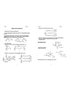
Transcription of W631GG6MB 8M 8 BANKS 16 BIT DDR3 SDRAM - Winbond
1 W631GG6MB 8M 8 BANKS 16 BIT ddr3 SDRAM Publication Release Date: Nov. 23, 2017 Revision: A02 - 1 - Table of Contents- 1. GENERAL DESCRIPTION .. 5 2. FEATURES .. 5 3. ORDER INFORMATION .. 6 4. KEY PARAMETERS .. 7 5. BALL CONFIGURATION .. 8 6. BALL DESCRIPTION .. 9 7. BLOCK DIAGRAM .. 11 8. FUNCTIONAL DESCRIPTION .. 12 Basic Functionality .. 12 RESET and Initialization Procedure .. 12 Power-up Initialization Sequence .. 12 Reset Initialization with Stable Power .. 14 Programming the Mode Registers .. 15 Mode Register MR0 .. 17 Burst Length, Type and Order .. 18 CAS 18 Test 19 DLL 19 Write Recovery .. 19 Precharge PD DLL .. 19 Mode Register MR1 .. 20 DLL Enable/Disable .. 20 Output Driver Impedance Control.
2 21 ODT RTT Values .. 21 Additive Latency (AL) .. 21 Write leveling .. 21 Output Disable .. 21 Mode Register MR2 .. 22 Partial Array Self Refresh (PASR) .. 23 CAS Write Latency (CWL) .. 23 Auto Self Refresh (ASR) and Self Refresh Temperature (SRT) .. 23 Dynamic ODT (Rtt_WR) .. 23 Mode Register MR3 .. 24 Multi Purpose Register (MPR) .. 24 No OPeration (NOP) Command .. 25 Deselect Command .. 25 DLL-off Mode .. 25 DLL on/off switching procedure .. 26 DLL on to DLL off Procedure .. 26 DLL off to DLL on Procedure .. 27 Input clock frequency change .. 28 Frequency change during 28 Frequency change during Precharge Power-down .. 28 Write Leveling .. 30 DRAM setting for write leveling & DRAM termination function in that mode.
3 31 W631GG6MB Publication Release Date: Nov. 23, 2017 Revision: A02 - 2 - Write Leveling Procedure .. 31 Write Leveling Mode Exit .. 33 Multi Purpose Register .. 34 MPR Functional Description .. 35 MPR Register Address Definition .. 36 Relevant Timing Parameters .. 36 Protocol Example .. 36 ACTIVE Command .. 42 PRECHARGE Command .. 42 READ Operation .. 43 READ Burst Operation .. 43 READ Timing Definitions .. 44 READ Timing; Clock to Data Strobe relationship .. 45 READ Timing; Data Strobe to Data relationship .. 46 tLZ(DQS), tLZ(DQ), tHZ(DQS), tHZ(DQ) Calculation .. 47 tRPRE Calculation .. 48 tRPST Calculation .. 48 Burst Read Operation followed by a 54 WRITE Operation .. 56 ddr3 Burst Operation.
4 56 WRITE Timing Violations .. 56 Motivation .. 56 Data Setup and Hold Violations .. 56 Strobe to Strobe and Strobe to Clock Violations .. 56 Write Timing Parameters .. 56 Write Data 57 tWPRE 58 tWPST Calculation .. 58 Refresh Command .. 65 Self-Refresh Operation .. 67 Power-Down Modes .. 69 Power-Down Entry and Exit .. 69 Power-Down clarifications - Case 1 .. 75 Power-Down clarifications - Case 2 .. 75 Power-Down clarifications - Case 3 .. 76 ZQ Calibration Commands .. 77 ZQ Calibration Description .. 77 ZQ Calibration Timing .. 78 ZQ External Resistor Value, Tolerance, and Capacitive loading .. 78 On-Die Termination (ODT) .. 79 ODT Mode Register and ODT Truth Table .. 79 Synchronous ODT Mode.
5 80 ODT Latency and Posted ODT .. 80 Timing Parameters .. 80 ODT during Reads .. 82 Dynamic ODT .. 83 Functional Description: .. 83 ODT Timing Diagrams .. 84 Asynchronous ODT Mode .. 88 W631GG6MB Publication Release Date: Nov. 23, 2017 Revision: A02 - 3 - Synchronous to Asynchronous ODT Mode Transitions .. 89 Synchronous to Asynchronous ODT Mode Transition during Power-Down Entry .. 89 Asynchronous to Synchronous ODT Mode Transition during Power-Down 92 Asynchronous to Synchronous ODT Mode during short CKE high and short CKE low periods 93 9. OPERATION MODE .. 94 Command Truth Table .. 94 CKE Truth Table .. 96 Simplified State Diagram .. 97 10. ELECTRICAL CHARACTERISTICS .. 98 Absolute Maximum Ratings.
6 98 Operating Temperature Condition .. 98 DC & AC Operating Conditions .. 98 Recommended DC Operating Conditions .. 98 Input and Output Leakage Currents .. 99 Interface Test Conditions .. 99 DC and AC Input Measurement Levels .. 100 DC and AC Input Levels for Single-Ended Command and Address Signals .. 100 DC and AC Input Levels for Single-Ended Data Signals .. 101 Differential swing requirements for clock (CK - CK#) and strobe (DQS - DQS#) .. 103 Single-ended requirements for differential signals .. 104 Differential Input Cross Point Voltage .. 105 Slew Rate Definitions for Single-Ended Input Signals .. 106 Slew Rate Definitions for Differential Input Signals .. 106 DC and AC Output Measurement Levels .. 107 Output Slew Rate Definition and Requirements.
7 107 Single Ended Output Slew Rate .. 108 Differential Output Slew Rate .. 109 34 ohm Output Driver DC Electrical Characteristics .. 110 Output Driver Temperature and Voltage sensitivity .. 112 On-Die Termination (ODT) Levels and Characteristics .. 113 ODT Levels and I-V Characteristics .. 113 ODT DC Electrical Characteristics .. 114 ODT Temperature and Voltage sensitivity .. 114 Design guide lines for RTTPU and RTTPD .. 115 ODT Timing 116 Test Load for ODT Timings .. 116 ODT Timing Definitions .. 116 Input/Output Capacitance .. 120 Overshoot and Undershoot 121 AC Overshoot /Undershoot Specification for Address and Control Pins: .. 121 AC Overshoot /Undershoot Specification for Clock, Data, Strobe and Mask pins.
8 121 IDD and IDDQ Specification Parameters and Test Conditions .. 122 IDD and IDDQ Measurement Conditions .. 122 IDD Current Specifications .. 132 Clock Specification .. 133 Speed Bins .. 134 ddr3 -1333 Speed Bin and Operating Conditions .. 134 ddr3 -1600 Speed Bin and Operating Conditions .. 135 ddr3 -1866 Speed Bin and Operating Conditions .. 136 W631GG6MB Publication Release Date: Nov. 23, 2017 Revision: A02 - 4 - ddr3 -2133 Speed Bin and Operating Conditions .. 137 Speed Bin General Notes .. 138 AC Characteristics .. 139 AC Timing and Operating Condition for -09/09I/09J/-11/11I/11J speed grades .. 139 AC Timing and Operating Condition for -12/12I/12J/-15/15I/15J speed grades .. 143 Timing Parameter Notes .. 147 Address / Command Setup, Hold and Derating.
9 150 Data Setup, Hold and Slew Rate Derating .. 157 11. PACKAGE SPECIFICATION .. 159 12. REVISION HISTORY .. 160 W631GG6MB Publication Release Date: Nov. 23, 2017 Revision: A02 - 5 - 1. GENERAL DESCRIPTION The W631GG6MB is a 1G bits ddr3 SDRAM , organized as 8,388,608 words 8 BANKS 16 bits. This device achieves high speed transfer rates up to 2133 MT/s ( ddr3 -2133) for various applications. This device is sorted into the following speed grades: -09, -11, -12, -15, 09I, 11I, 12I, 15I, 09J, 11J, 12J and 15J. The -09 ,09I and 09J speed grades are compliant to the ddr3 -2133 (14-14-14) specification (The 09I industrial grade which is guaranteed to support -40 C TCASE 95 C, the 09J industrial plus grade which is guaranteed to support -40 C TCASE 105 C).
10 The -11 ,11I and 11J speed grades are compliant to the ddr3 -1866 (13-13-13) specification (The 11I industrial grade which is guaranteed to support -40 C TCASE 95 C, the 11J industrial plus grade which is guaranteed to support -40 C TCASE 105 C). The -12, 12I and 12J speed grades are compliant to the ddr3 -1600 (11-11-11) specification (The 12I industrial grade which is guaranteed to support -40 C TCASE 95 C, the 12J industrial plus grade which is guaranteed to support -40 C TCASE 105 C). The -15, 15I and 15J speed grades are compliant to the ddr3 -1333 (9-9-9) specification (The 15I industrial grade which is guaranteed to support -40 C TCASE 95 C, the 15J industrial plus grade which is guaranteed to support -40 C TCASE 105 C).