Transcription of Wide Supply Dual, 17 MHz, Rail-to-Rail FET Input Amplifier ...
1 wide Supply Dual, 17 MHz, rail -to-RailFET Input AmplifierData sheet ad823a Rev. B Information furnished by analog devices is believed to be accurate and reliable. However, no responsibility is assumed by analog devices for its use, nor for any infringements of patents or other rights of third parties that may result from its use. Specifications subject to change without notice. No license is granted by implication or otherwise under any patent or patent rights of analog devices .
2 Trademarks and registered trademarks are the property of their respective owners. One Technology Way, Box 9106, Norwood, MA 02062-9106, : Fax: 2012 analog devices , Inc. All rights reserved. FEATURES Single- Supply operation Output swings Rail-to-Rail Input voltage range extends below ground Single- Supply capability from 3 V to 36 V High load drive Capacitive load drive of 470 pF (G = +1, 25% overshoot) Linear output current of 40 mA, V from supplies Excellent ac performance on mA/ Amplifier 3 dB bandwidth of 17 MHz, G = +1 325 ns settling time to (2 V step) Slew rate of 30 V/ s Low distortion.
3 108 dBc at 20 kHz (G = 1, RL = 2 k ) Good dc performance 700 V maximum Input offset voltage 1 V/ C offset voltage drift 25 pA maximum Input bias current Low noise: 14 nV/ Hz at 10 kHz No phase inversion with inputs to the Supply rails APPLICATIONS Photodiode preamps Active filters 12-bit to 16-bit data acquisition systems Medical instrumentation Precision instrumentation GENERAL DESCRIPTION The ad823a is a dual precision, 17 MHz, JFET Input op amp manufactured in the extra fast complementary bipolar (XFCB) process.
4 The ad823a can operate from a single Supply of 3 V to 36 V or from dual supplies of V to 18 V. It has true single- Supply capability with an Input voltage range extending below ground in single- Supply mode. Output voltage swing extends to within 20 mV of each rail for IOUT 100 A, providing outstanding output dynamic range. It also has a linear output current of 40 mA, V from the Supply rails. An offset voltage of 700 V maximum, an offset voltage drift of 1 V/ C, and typical Input bias currents of pA provide dc precision with source impedances up to 1 G.
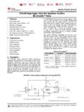
5 The ad823a provides 17 MHz, 3 dB bandwidth, and a 30 V/ s slew rate with a low Supply current of only mA per Amplifier . It also provides low Input voltage noise of 14 nV/ Hz and 108 dB SFDR at 20 kHz. The ad823a has low Input capacitances ( pF differ-ential and pF common mode) and drives more than 500 pF of direct capacitive load as a follower. This lets the Amplifier handle a wide range of load conditions. CONNECTION DIAGRAM AD823 AOUT1+IN2 IN2 OUT2+VS IN1+IN1 VS1234876509439-001 Figure 1.
6 8-Lead SOIC 09439-102 OUT11 IN12+IN13 VS4+VS8 OUT27 IN26+IN25AD823 ATOP VIEW(Not to Scale) Figure 2. 8-Lead MSOP 200 s/DIV500 = 3 VCL = 50pFG = +1 Figure 3. Output Swing, +VS = +3 V, G = +1 This combination of ac and dc performance, plus the outstanding load drive capability, results in an exceptionally versatile ampli-fier for applications such as ADC drivers, high speed active filters, and other low voltage, high dynamic range systems. The ad823a is available over the industrial temperature range of 40 C to +85 C and is offered in an 8-lead SOIC package and an 8-lead MSOP package.
7 ad823a data sheet Rev. B | Page 2 of 20 TABLE OF CONTENTS Features .. 1 Applications .. 1 General Description .. 1 Connection Diagram .. 1 Revision History .. 2 Specifications .. 3 5 V Operation .. 3 V Operation .. 4 15 V Operation .. 5 Absolute Maximum Ratings .. 6 Thermal Resistance .. 6 ESD Caution .. 6 Pin Configuration and Function Descriptions ..7 Typical Performance Characteristics ..8 Theory of Operation .. 14 Output Impedance .. 14 Applications Information .. 15 Input Characteristics.
8 15 Output 15 Wideband Photodiode Preamp .. 16 Active Filter .. 18 Maximizing Performance Through Proper Layout .. 19 Outline Dimensions .. 20 Ordering Guide .. 20 REVISION HISTORY 6/12 Rev. A to Rev. B Added Text to Absolute Maximum Ratings Section .. 6 Changes to Equation 8 .. 18 5/12 Revision A: Initial Version data sheet ad823a Rev. | Page 3 of 20 SPECIFICATIONS 5 V OPERATION TA = 25 C, +VS = 5 V, RL = 2 k to V, unless otherwise noted. Table 1. Parameter Conditions Min Typ Max Unit DYNAMIC PERFORMANCE 3 dB Bandwidth G = +1, VOUT V p-p 17 MHz Full Power Response VOUT = 2 V p-p MHz Slew Rate G = 1, VOUT = 4 V step 25 30 V/ s Settling Time To G = 1, VOUT = 2 V step 240 ns To G = 1, VOUT = 2 V step 325 ns NOISE/DISTORTION PERFORMANCE Input Voltage Noise f = 10 kHz 14 nV/ Hz Input Current Noise f = 1 kHz 1 fA/ Hz Harmonic Distortion (SFDR)
9 VOUT = 2 V p-p, f = 20 kHz, G = 1, RF = RG = 4 k 108 dBc VOUT = 2 V p-p, f = 20 kHz, G = +1, RL = 1 k 99 dBc Crosstalk f = 1 kHz RL = 5 k 123 dB f = 1 MHz RL = 5 k 77 dB DC PERFORMANCE Initial Offset mV Maximum Offset ove r Temperature mV Offset Drift 1 V/ C Input Bias Current VCM = 0 V to 4 V 25 pA At TMAX VCM = 0 V to 4 V 10 25 pA Input Offset Current 20 pA At TMAX pA Open-Loop Gain VOUT = V to 4 V, RL = 2 k 40 175 V/mV TMIN to TMAX 25 V/mV Input CHARACTERISTICS Input Common-Mode Voltage Range to +3 to + V Input Resistance 1013 Input Capacitance Differential Mode pF Common Mode pF Common-Mode Rejection Ratio VCM = 0 V to 3 V 60 73 dB OUTPUT CHARACTERISTICS Output Voltage Swing IL = 100 A to V IL = 2 mA to V IL = 10 mA to V Linear Output Current VOUT = V to V 40 mA Short-Circuit Current Sourcing to V 50 mA
10 Sinking to V 101 mA Capacitive Load Drive G = +1 500 pF POWER Supply Operating Range 3 36 V Quiescent Current TMIN to TMAX, total mA Power Supply Rejection Ratio VS = 5 V to 15 V, TMIN to TMAX 70 94 dB BAD823A data sheet Rev. | Page 4 of 20 V OPERATION TA = 25 C, +VS = V, RL = 2 k to V, unless otherwise noted. Table 2. Parameter Conditions Min Typ Max Unit DYNAMIC PERFORMANCE 3 dB Bandwidth G = +1, VOUT V p-p, VCM = V MHz Full Power Response VOUT = 2 V p-p MHz Slew Rate G = 1, VOUT = 2 V step, VCM = V 18 23 V/ s Settling Time To G = 1, VOUT = 2 V step 350 ns To G = 1, VOUT = 2 V step 460 ns NOISE/DISTORTION PERFORMANCE Input Voltage Noise f = 10 kHz 14 nV/ Hz Input Current Noise f = 1 kHz 1 fA/ Hz Harmonic Distortion (SFDR)