Transcription of Wien-bridge oscillator with low harmonic distortion
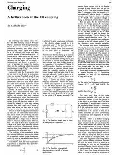
1 WIRELESS WORLD MAY 1981 Wien-bridge oscillator with low harmonic distortion New way of using Wien network to give % by J. L. Linsley Hood, Robins (Electronics) 1kHz of some , which tended to increase with frequency above this point, as the effectiveness of the common-mode isolation deteriorated. R 51 The Wien-bridge network can be connected in a different way in an oscillator circuit to give a sine wave with very low total harmonic distortion . An amplitude control is external to the circuit. However, it is not implicit, in the use of a Wien network as the frequency-control method, that the configuration shown in Fig. 1, in which the output of the network is taken to the non-inverting input of the amplifier and the amplitude controlling negative-feedback signal is taken to the other, is the only circuit configuration which can be employed.
2 In particular, con sideration of the phase and transmission characteristics of such a network, shown in Table 1 and Fig. 2 for equal values of C Output The Wien-bridge network remains the most popular method of construction of variable-frequency sine-wave oscillators , since the basic circuit can be very simple in form. It is a fairly straightforward matter to design oscillators of this type in which the harmonic distortion is only of the order of , and which allow frequency control by means of a simple 2-gang poten tiometer. The basic circuit for an oscillator of this form, using a single operational amplifier as the gain block, is shown in Fig. 1, and the author has shown a practical design of oscillator , based on this, for a use as a simple, general-purpose workshop tool.
3 1 However, in the form shown in Fig. 1, a significant problem exists in that the trans mission of a normal Wien network, at the operating frequency, is only 113, which means that an inconveniently large propor tion of the output signal voltage appears at the inputs of the amplifier, and will lead to non-linearities in the transfer characteris tics of the amplifier due to 'common mode' defects. An oscillator design, which em ployed an input device operated in a cas code configuration with a junction t. to minimize this type of defect, was shown by the author in 1977,6 and allowed a at TABLE 1. Phase and transmission charac teristics of simple Wien network.
4 FIFa phase transmission " 0 " 2 " 3 5 8 10. R ov Fig. 1. Basic Wien-bridge oscillator circuit Fig. 2. Gain and phase characteristics of Wien network R '--ov (al Ibl R R z 1-0 O o O 9 8 7 l O 6 Vl i: O Vl O 0: f-O. O O " 4 3 2 1 0 131 z 0 w_ >Vl _Vl i: -IVl 121 wz 0: 0: .. 111 ,/7 " ..z --'/}:;II)' / ' I 01 02 04 0 6 0 2 4 OSCILLATION FREQUENCY Fig. 3. Rearrangement of Wien network between signal sources gives small in phase signal at point X Fig. 4. Use of arrangement of Fig. 3 in oscillator circuit Outr>ut I-Eyl ----4 ------- -------_OV Figures in brackets refer to diagram 3 b 0 -w Vl ;!
5 CL 9Cf' 52 and R, implies that if, instead of the net work of Fig. 3(a) being connected between a signal source Ein and the OV line, it was connected between two signal sources + E x and -Ey, where these are sinusoidal and identical in frequency and the negative sign implies phase opposition, as shown in Fig. 3(b), then a small, in-phase signal would exist at the point 'X', at the fre quency of maximum transmission, (fo), if +Ex was slightly greater than -2Ey This could then be used as a positive feedback signal in a circuit such as that shown in Fig. 4, to sustain oscillation at the frequency fo. Indeed, such a circuit will work quite well, and will sustain a constant output magnitude of oscillation if a thermistor is employed, as shown, to make the gain of the second, inverting, amplifier stage dependent on the ampli tude of the input signal.
6 However, there is, in practice, a small snag with such an arrangement, and that is that the inverted negative-feedback signal applied to the in put of Al will suffer an additional phase error due to the internal time lag within A2, and this will cause unwanted insta bility if '3rd generation' high speed op. amps. such as the CA 3140, or the 1741 S, are used in the realisation of this circuit. It is, fortunately, an easy matter to re solve this difficulty if the circuit is recast in the form shown in Fig. 5, in which the negative-feedback signal, equivalent to -Ey in Fig. 3(b), is derived from the am plifier AI> and the positive-feedback signal is obtained from the output of the second inverting amplifier A2 This configuration offers several signifi cant advantages.
7 The input signal to Al is extremely small, since it is only required to be EOUl/2M, where M is the open-loop gain of A I -typically 100dB for a good modern - and, as pointed out by the author in an earlier article2, with semi conductor amplifiers the non-linearity of such devices is essentially an input charac teristic, dependent on the magnitude of the input signal. The second-stage amplifier is operated as a shunt-feedback element, and the non linearities of such a stage can be shown to be significantly lower, because of the very small input-signal amplitude and the ab sence of any internal transfer errors be tween the inverting and non-inverting in puts, than is the case for an identical amplifying element in a series-feedback configuration.
8 3,4 The time-delay errors in the second am plifying stage (A2) no longer contribute to loss of stablility in the system, but only to a very small compensatory shift in the R R WIRELESS WORLD MAY 1981 operating frequency of the oscillator . Fast response-speed, high gain can therefore be used without problems. For these reasons, it can be expected that the residual harmonic distortion of this oscillator design will be exceedingly small, and measurements on two proto types have indeed shown this to be the case. So far as can be determined, the residual distortion - almost exclusively Thermistor Rs Output ____ -------------- ------------ OV Figures in brackets refer to diagnom 3b Rp.
9 Rs and Rin chosen to SUIt individual thermistor employed Fig. 5. Final form of new configuration in low- distortion oscillator :z o 0 01 009 005 0001 o l V) a .0005 00001 100 , (Includes ,50 Hz "hum" I " "-, " .. ---lk 1 Ok FREQUENCY (Hz) Fig. 6. Measured total harmonic distortion of improved oscillator of Fig. 5 Fig. 7. New oscillator with external optoelectronic amplitude-control circuit. Silonex (formerly National Semiconductors) cell, Type NSL395, is obtainable from Cheston Electronics Ltd., Vanguard House, 56 Oughton Street, Ormskirk, Lancs. Tel: 069572456 1/ Photoconductive cell 10k NSL395 47k \ -------------- vr-------------- / oscillator Output Si Si 3k3 Si 3k3 3k3 3k3 \ ------------------ vr------------------ / Full wave rectifier Note: PC1 and LED1 are in optical contact 10}!
10 56k I1 \ ------,v ---- / Feedback control circuit WIRELESS WORLD MAY 1981 third harmonic - is that due to the de pendence of the resistance of the thermis tors used to control the amplitude of the oscillation on the instantaneous value of the signal potential applied to them. This characteristic of oscillators with averaging control s stems has been analysed by Robinson who suggests that the distortion of such a system, which is shown to be mainly third harmonic , will be X3 _ 1 Ao-l'j 1 Xl - 8rj . -l'j-. 'Iitji where (Ao-l'j)/l'j is the fraction by which the low-level loop gain exceeds the gain required to initiate oscillation, and T is the time constant of the control system (ther mistor or similar).