Transcription of Xilinx DS610 Spartan-3A DSP FPGA Family, Data Sheet
1 DS610 October 4, Specification1 Copyright 2007 2010 Xilinx , Inc. Xilinx , the Xilinx logo, Virtex, spartan , ISE, and other designated brands included herein are trademarks of Xilinx in the United States and other countries. PCI and PCI-X are trademarks of PCI-SIG and used under license. All other trademarks are the property of their respective 1: Introduction and Ordering InformationDS610 ( ) October 4, 2010 Introduction Features Architectural Overview Configuration Overview General I/O Capabilities Supported Packages and Package Marking Ordering InformationModule 2:Functional DescriptionDS610 ( ) October 4, 2010 The functionality of the spartan -3A DSP FPGA family is described in the following documents. UG331: spartan -3 Generation FPGA User Guide Clocking Resources Digital Clock Managers (DCMs) Block RAM Configurable Logic Blocks (CLBs)-Distributed RAM-SRL16 Shift Registers-Carry and Arithmetic Logic I/O Resources Programmable Interconnect ISE Software Design Tools and IP Cores Embedded Processing and Control Solutions Pin Types and Package Overview Package Drawings Powering fpgas Power Management UG332.
2 spartan -3 Generation Configuration User Guide Configuration Overview Configuration Pins and Behavior Bitstream Sizes Detailed Descriptions by Mode-Master Serial Mode using Platform Flash PROM-Master SPI Mode using Commodity Serial Flash-Master BPI Mode using Commodity Parallel Flash-Slave Parallel (SelectMAP) using a Processor-Slave Serial using a Processor-JTAG Mode ISE iMPACT Programming Examples MultiBoot Reconfiguration Design Authentication using Device DNA UG431: XtremeDSP DSP48A for Spartan-3A DSP fpgas User Guide DSP48A Slice Design Considerations DSP48A Architecture Highlights-18 x 18-Bit Multipliers-48-Bit Accumulator-18-bit Pre-Adder DSP48A Application ExamplesModule 3: DC and Switching CharacteristicsDS610 ( ) October 4, 2010 DC Electrical Characteristics Absolute Maximum Ratings Supply Voltage Specifications Recommended Operating Conditions Switching Characteristics I/O Timing Configurable Logic Block (CLB) Timing Digital Clock Manager (DCM) Timing Block RAM Timing XtremeDSP Slice Timing Configuration and JTAG TimingModule 4: Pinout DescriptionsDS610 ( ) October 4, 2010 Pin Descriptions Package Overview Pinout Tables Footprint Diagrams1 Spartan-3A DSP FPGA Family Data SheetDS610 October 4, 2010 Product SpecificationDS610 ( ) October 4, Specification2 Copyright 2007 2010 Xilinx , Inc.
3 Xilinx , the Xilinx logo, Virtex, spartan , ISE, and other designated brands included herein are trademarks of Xilinx in the United States and other countries. PCI and PCI-X are trademarks of PCI-SIG and used under license. All other trademarks are the property of their respective spartan -3A DSP family of Field-Programmable Gate Arrays ( fpgas ) solves the design challenges in most high- volume, cost-sensitive, high-performance DSP applications. The two-member family offers densities ranging from to million system gates, as shown in Ta b l e Spartan-3A DSP family builds on the success of the Spartan-3A FPGA family by increasing the amount of memory per logic and adding XtremeDSP DSP48A slices. New features improve system performance and reduce the cost of configuration. These Spartan-3A DSP FPGA enhancements, combined with proven 90 nm process technology, deliver more functionality and bandwidth per dollar than ever before, setting the new standard in the programmable logic and DSP processing Spartan-3A DSP fpgas extend and enhance the Spartan-3A FPGA family.
4 The XC3SD1800A and the XC3SD3400A devices are tailored for DSP applications and have additional block RAM and XtremeDSP DSP48A slices. The XtremeDSP DSP48A slices replace the 18x18 multipliers found in the Spartan-3A devices and are based on the DSP48 blocks found in the Virtex -4 devices. The block RAMs are also enhanced to run faster by adding an output register. Both the block RAM and DSP48A slices in the Spartan-3A DSP devices run at 250 MHz in the lowest cost, standard -4 speed of their exceptional DSP price/performance ratio, Spartan-3A DSP fpgas are ideally suited to a wide range of consumer electronics applications, such as broadband access, home networking, display/projection, and digital Spartan-3A DSP family is a superior alternative to mask programmed ASICs. fpgas avoid the high initial cost, lengthy development cycles, and the inherent inflexibility of conventional ASICs.
5 Also, FPGA programmability permits design upgrades in the field with no hardware replacement necessary, an impossibility with Very low cost, high-performance DSP solution for high-volume, cost-conscious applications 250 MHz XtremeDSP DSP48A Slices Dedicated 18-bit by 18-bit multiplier Available pipeline stages for enhanced performance of at least 250 MHz in the standard -4 speed grade 48-bit accumulator for multiply-accumulate (MAC) operation Integrated adder for complex multiply or multiply-add operation Integrated 18-bit pre-adder Optional cascaded Multiply or MAC Hierarchical SelectRAM memory architecture Up to 2268 Kbits of fast block RAM with byte write enables for processor applications Up to 373 Kbits of efficient distributed RAM Registered outputs on the block RAM with operation of at least 280 MHz in the standard -4 speed grade Dual-range VCCAUX supply simplifies design Suspend, Hibernate modes reduce system power Low-power option reduces quiescent current Multi-voltage, multi-standard SelectIO interface pins Up to 519 I/O pins or 227 differential signal pairs LVCMOS, LVTTL, HSTL, and SSTL single-ended I/O , , , , and signaling Selectable output drive.
6 Up to 24 mA per pin QUIETIO standard reduces I/O switching noise Full 10% compatibility and hot swap compliance 622+ Mb/s data transfer rate per differential I/O LVDS, RSDS, mini-LVDS, HSTL/SSTL differential I/O with integrated differential termination resistors Enhanced Double Data Rate (DDR) support DDR/DDR2 SDRAM support up to 333 Mb/s Fully compliant 32-/64-bit, 33/66 MHz PCI support Abundant, flexible logic resources Densities up to 53712 logic cells, including optional shift register Efficient wide multiplexers, wide logic, fast carry logic IEEE JTAG programming/debug port Eight Digital Clock Managers (DCMs) Clock skew elimination (delay locked loop) Frequency synthesis, multiplication, division High-resolution phase shifting Wide frequency range (5 MHz to over 320 MHz) Eight low-skew global clock networks, eight additional clocks per half device, plus abundant low-skew routing Configuration interface to industry-standard PROMs Low-cost, space-saving SPI serial Flash PROM x8 or x8/x16 BPI parallel NOR Flash PROM Low-cost Xilinx Platform Flash with JTAG Unique Device DNA identifier for design authentication Load multiple bitstreams under FPGA control Post-configuration CRC checking MicroBlaze and PicoBlaze embedded processor cores BGA and CSP packaging with Pb-free options Common footprints support easy density migration XA Automotive version available6 Spartan-3A DSP FPGA Family:Introduction and Ordering InformationDS610 ( ) October 4, 2010 Product SpecificationTable 1.
7 Summary of Spartan-3A DSP FPGA AttributesDeviceSystem GatesEquivalent Logic CellsCLB Array (One CLB = Four Slices)Distributed RAMBits(1)Block RAM Bits(1)DSP48As DCMsMaximum User I/OMaximum Differential I/O PairsRows ColumnsTotalCLBsTotalSlicesXC3SD1800A180 0K37,44088484,16016,640260K1512K84851922 7XC3SD3400A3400K53,712104585,96823,87237 3K2268K1268469213 Notes: convention, one Kb is equivalent to 1,024 DSP FPGA Family: Introduction and Ordering InformationDS610 ( ) October 4, Specification3 Architectural OverviewThe Spartan-3A DSP family architecture consists of five fundamental programmable functional elements: XtremeDSP DSP48A Slice provides an 18-bit x 18-bit multiplier, 18-bit pre-adder, 48-bit post-adder/accumulator, and cascade capabilities for various DSP applications. Block RAM provides data storage in the form of 18-Kbit dual-port blocks.
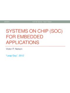
8 Configurable Logic Blocks (CLBs) contain flexible Look-Up Tables (LUTs) that implement logic plus storage elements used as flip-flops or latches. CLBs perform a wide variety of logical functions as well as store data. Input/Output Blocks (IOBs) control the flow of data between the I/O pins and the internal logic of the device. IOBs support bidirectional data flow plus 3-state operation. Supports a variety of signal standards, including several high-performance differential standards. Double Data-Rate (DDR) registers are included. Digital Clock Manager (DCM) Blocks provide self-calibrating, fully digital solutions for distributing, delaying, multiplying, dividing, and phase-shifting clock elements are organized as shown in Figure 1. A dual ring of staggered IOBs surrounds a regular array of CLBs. The XC3SD1800A has four columns of DSP48As, and the XC3SD3400A has five columns of DSP48As.
9 Each DSP48A has an associated block RAM. The DCMs are positioned in the center with two at the top and two at the bottom of the device and in the two outer columns of the 4 or 5 columns of block RAM and Spartan-3A DSP family features a rich network of routing that interconnect all five functional elements, transmitting signals among them. Each functional element has an associated switch matrix that permits multiple connections to the Target - Figure 1 Figure 1: Spartan-3A DSP Family ArchitectureCLBB lock RAMDCMIOBsIOBsDS610-1_01_031207 IOBsIOBsDCMB lock RAM / DSP48A SliceDCMCLBsIOBsDSP48A SliceNotes: XC3SD1800A and XC3SD3400A have two DCMs on both the left and right sides, as well as the two DCMs at the top and bottom of the devices. The two DCMs on the left and right of the chips are in the middle of the outer Block RAM/DSP48A columns of the 4 or 5 columns in the selected device, as shown in the diagram detailed diagram of the DSP48A can be found in UG431: XtremeDSP DSP48A for Spartan-3A DSP fpgas User DSP FPGA Family: Introduction and Ordering InformationDS610 ( ) October 4, Specification4 ConfigurationSpartan-3A DSP fpgas are programmed by loading configuration data into robust, reprogrammable, static CMOS configuration latches (CCLs) that collectively control all functional elements and routing resources.
10 The FPGA s configuration data is stored externally in a PROM or some other non-volatile medium, either on or off the board. After applying power, the configuration data is written to the FPGA using any of seven different modes: Master Serial from a Xilinx Platform Flash PROM Serial Peripheral Interface (SPI) from an industry-standard SPI serial Flash Byte Peripheral Interface (BPI) Up from an industry-standard x8 or x8/x16 parallel NOR Flash Slave Serial, typically downloaded from a processor Slave Parallel, typically downloaded from a processor Boundary Scan (JTAG), typically downloaded from a processor or system testerFurthermore, Spartan-3A DSP fpgas support MultiBoot configuration, allowing two or more FPGA configuration bitstreams to be stored in a single SPI serial Flash or a BPI parallel NOR Flash.