Transcription of ZedBoard HW Users Guide
1 ZedBoard (Zynq Evaluation and Development) Hardware User s Guide Version 2. 2 27 January 2014 Table of Contents 1 INTRODUCTION .. 2 ZYNQ BANK PIN ASSIGNMENTS .. 4 2 FUNCTIONAL DESCRIPTION .. 5 ALL PROGRAMMABLE SOC .. 5 MEMORY .. 5 DDR3 .. 5 SPI Flash .. 7 SD Card Interface ..10 USB ..11 USB OTG ..11 USB-to-UART Bridge ..11 USB-JTAG ..12 USB circuit protection ..13 DISPLAY AND AUDIO ..13 HDMI Output ..13 VGA I2S Audio Codec ..17 OLED ..18 CLOCK SOURCES ..18 RESET SOURCES ..18 Power on Reset (PS_POR_B) ..18 Program Push Button Switch.
2 19 Processor Subsystem Reset ..19 USER I/O ..19 User Push Buttons ..19 User DIP Switches ..19 User LEDs ..20 10/100/1000 ETHERNET PHY ..20 EXPANSION HEADERS ..21 LPC FMC Connector ..21 Digilent Pmod Compatible Headers (2x6)..22 Agile Mixed Signaling (AMS) Connector, J2 ..23 CONFIGURATION MODES ..26 JTAG ..27 POWER ..28 Primary Power Input ..28 On/Off Switch ..28 Regulators ..28 Sequencing ..29 Power Good LED ..30 Power Estimation ..30 Testing ..31 Probes ..31 3 ZYNQ-7000 AP SOC BANKS ..32 ZYNQ-7000 AP SOC BANK VOLTAGES ..33 4 JUMPER SETTINGS.
3 34 5 MECHANICAL ..36 6 REVISION HISTORY ..37 27-Jan-2014 1 1 Introduction The ZedBoard is an evaluation and development board based on the Xilinx ZynqTM-7000 All Programmable SoC (AP SoC). Combining a dual Corex-A9 Processing System (PS) with 85,000 Series-7 Programmable Logic (PL) cells, the Zynq-7000 AP SoC can be targeted for broad use in many applications. The ZedBoard s robust mix of on-board peripherals and expansion capabilities make it an ideal platform for both novice and experienced designers. The features provided by the ZedBoard consist of: Xilinx XC7Z020-1 CLG484C Zynq-7000 AP SoC o Primary configuration = QSPI Flash o Auxiliary configuration options Cascaded JTAG SD Card Memory o 512 MB DDR3 (128M x 32) o 256 Mb QSPI Flash Interfaces o USB-JTAG Programming using Digilent SMT1-equivalent circuit Accesses PL JTAG PS JTAG pins connected through PS Pmod o 10/100/1G Ethernet o USB OTG o SD Card o USB FS USB-UART bridge o Five Digilent Pmod compatible headers (2x6) (1 PS, 4 PL) o One LPC FMC o One AMS Header o Two Reset Buttons (1 PS, 1 PL) o Seven Push Buttons (2 PS, 5 PL)
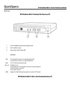
4 O Eight dip/slide switches (PL) o Nine User LEDs (1 PS, 8 PL) o DONE LED (PL) On-board Oscillators o MHz (PS) o 100 MHz (PL) Display/Audio o HDMI Output o VGA (12-bit Color) o 128x32 OLED Display o Audio Line-in, Line-out, headphone, microphone Power o On/Off Switch o 12V @ 5A AC/DC regulator Software o ISE WebPACK Design Software o License voucher for ChipScope Pro locked to XC7Z020 27-Jan-2014 2 ZYNQ XC7Z020-CLG484 DDR3 MIC InLine InLine OutHdPhn Out32 PmodsQSPI7 PmodFlash814 GbitEnet12 USBOTG8SD21 LED,2 buttonsUSBContUSBUART3714 USBContClkFMC-LPCGPIO (8 LEDs,8 slide switches,5 pushbuttons)Type AHDMI Out8221827105 VGA (12-bit color)128x32 OLEDPHY1133 MhzResetPrimary JTAG512 Mbyte DDR3 (x32) Multiplexed I/O (MIO)Processing System (PS)
5 Programmable Logic (PL)1 PROGD isplayDDRPS_RSTJTAGPS_CLK<User Select>ENET/MDIOUSBOTGSDUSBUARTPS_GPIOQSPII2S/A CDGPIOFMCPMODHDMIVGAOLEDPROGPHYHDMI transmitterI2S AudioCodecXADC8 GPIO/VP/VN1 DONE LEDDONEClk100 Mhz1 GCLK Figure 1 ZedBoard Block Diagram 27-Jan-2014 3 Zynq Bank Pin Assignments The following figure shows the Zynq bank pin assignments on the ZedBoard followed by a table that shows the detailed I/O connections. Figure 2 - Zynq Z7020 CLG484 Bank Assignments 27-Jan-2014 4 2 Functional Description All Programmable SoC The ZedBoard features a Xilinx Zynq XC7Z020-1 CLG484 All Programmable SoC (AP SoC).
6 Initial ZedBoards were marked Rev C and shipped with Engineering Sample "CES" grade silicon. Later Rev D shipments switched to production "C" grade silicon once those became available. The Zynq-7000 AP SoC part markings indicate the silicon grade. Memory Zynq contains a hardened PS memory interface unit. The memory interface unit includes a dynamic memory controller and static memory interface modules. DDR3 The ZedBoard includes two Micron DDR3 128 Megabit x 16 memory components creating a 32-bit interface, totaling 512 MB. Earlier ZedBoards used Micron MT41J128M16HA-15E:D, but As of August 2012, this device has been marked by Micron for end-of-life.
7 There are several options that Micron offers for a replacement. ZedBoard will likely migrate to the MT41K128M16JT-125 device, although this is pending validation. The DDR3 is connected to the hard memory controller in the Processor Subsystem (PS) as outlined in the Zynq datasheet. The multi-protocol DDR memory controller is configured for 32-bit wide accesses to a 512 MB address space. The PS incorporates both the DDR controller and the associated PHY, including its own set of dedicated I/Os. DDR3 memory interface speeds up to 533 MHz (1066 Mbs) are supported. The DDR3 uses SSTL-compatible inputs.
8 DDR3 Termination is utilized on the ZedBoard . The Zynq-7000 AP SoC and DDR3 have been placed close together keeping traces short and matched. DDR3 on the PS was routed with 50 ohm targeted trace impedance for single-ended signals, and DCI resistors (VRP/VRN) as well as differential clocks set to 80 ohms. Each DDR3 chip needs its own 240-ohm pull-down on ZQ. The Xilinx Zynq-7000 All Programmable SoC PCB Design and Pin Planning Guide (UG933) recommends using 40 ohm trace impedance for DDR3 single-ended signals, so designers looking to duplicate the ZedBoard design may want consider this in their own board design.
9 See the appropriate ZedBoard Errata document for more details. DDR-VDDQ is set to to support the DDR3 devices selected. DDR-VTT is the termination voltage which is DDR-VDDQ. DDR-VREF is a separate buffered output that is equal to nominal DDR-VDDQ. The DDR-VREF is isolated to provide a cleaner reference for the DDR level transitions. 27-Jan-2014 5 The PCB design guidelines outlined in Zynq datasheet must be followed for trace matching, etc. Table 1 - DDR3 Connections Signal Name Description Zynq pin DDR3 pin DDR_CK_P Differential clock output N4 J7 DDR_CK_N Differential clock output N5 K7 DDR_CKE Clock enable V3 K9 DDR_CS_B Chip select P6 L2 DDR_RAS_B RAS row address select R5 J3 DDR_CAS_B RAS column address select P3 K3 DDR_WE_B Write enable R4 L3 DDR_BA[2:0] Bank address PS_DDR_BA[2:0] BA[2:0] DDR_A[14:0] Address PS_DDR_A[14:0] A[14:0] DDR_ODT Output dynamic termination P5 K1 DDR_RESET_B Reset F3 T2 DDR_DQ[31:0] I/O Data PS_DDR_[31:0] DDR3_DQ pins DDR_DM[3:0] Data mask PS_DDR_DM[3.]
10 0] LDM/UDM x2 DDR_DQS_P[3:0] I/O Differential data strobe PS_DDR_DQS_P[3:0] UDQS/LDQS DDR_DQS_N[3:0] I/O Differential data strobe PS_DDR_DQS_N[3:0] UDQS#/LDQS# DDR_VRP I/O Used to calibrate input termination N7 N/A DDR_VRN I/O Used to calibrate input termination M7 N/A DDR_VREF[1:0] I/O Reference voltage H7, P7 H1 For best DDR3 performance, DRAM training is enabled for write leveling, read gate, and read data eye options in the PS Configuration Tool in Xilinx Platform Studio (XPS) or the IP Editor in Vivado. Two entries allow for DQS to Clock Delay and Board Delay information to be specified for each of the four byte lanes.