Transcription of ZXM61P03F 30V P-channel enhancement mode MOSFET …
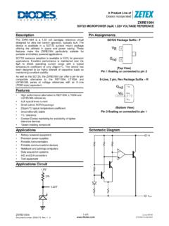
1 1 SEMICONDUCTORSZXM61P03 FISSUE 1 - OCTOBER 200530V P-channel enhancement MODE MOSFETSUMMARYV(BR)DSS=-30V; RDS(ON)= ; ID= new generation of high density mosfets from Zetex utilizes a uniquestructure that combines the benefits of low on-resistance with fast switchingspeed. This makes them ideal for high efficiency, low voltage, powermanagement Low on-resistance Fast switching speed Low threshold Low gate drive SOT23 packageAPPLICATIONS DC - DC converters Power management functions Disconnect switches Motor controlORDERING INFORMATIONDEVICEREEL SIZE(inches)TAPE WIDTH(mm)QUANTITYPER REELZXM61P03 FTA78 embossed3,000 ZXM61P03 FTC138 embossed10,000 DEVICE MARKINGP03 SOT23 Pin outTop viewZXM61P03 FSEMICONDUCTORSISSUE 1 - OCTOBER 20052 THERMAL RESISTANCEPARAMETERSYMBOLVALUEUNITJ unction to Ambient (a)R JA200 C/WJunction to Ambient (b)
2 R JA155 C/WNOTES:(a) For a device surface mounted on 25mm x 25mm FR4 PCB with high coverage of single sided 1oz copper, in still air conditions(b) For a device surface mounted on FR4 PCB measured at t 5 secs.(c) Repetitive rating - pulse width limited by maximum junction temperature. Refer to Transient Thermal Impedance MAXIMUM RATINGSPARAMETERSYMBOLLIMITUNITD rain-Source VoltageVDSS-30 VGate- Source VoltageVGS 20 VContinuous Drain Current(VGS=-10V; TA=25 C)(b)(VGS=-10V; TA=70 C)(b) Drain Current (c) Source Current (Body Diode)(b) Source Current (Body Diode)(c) Dissipation at TA=25 C (a)Linear Derating FactorPD6255mWmW/ CPower Dissipation at TA=25 C (b)Linear Derating COperating and Storage Temperature RangeTj:Tstg-55 to +150 CZXM61P03 FSEMICONDUCTORSISSUE 1 - OCTOBER 20053 CHARACTERISTICSZXM61P03 FSEMICONDUCTORSISSUE 1 - OCTOBER 20054 ELECTRICAL CHARACTERISTICS (at Tamb= 25 C unless otherwise stated).
3 UNIT Breakdown VoltageV(BR)DSS-30 VID=-250 A, VGS=0 VZero Gate Voltage Drain CurrentIDSS-1 AVDS=-30V, VGS=0 VGate-Body LeakageIGSS 100nAVGS= 20V, VDS=0 VGate-Source Threshold VoltageVGS(th) A, VDS=VGSS tatic Drain-Source On-State Resistance (1) RDS(on) VGS=-10V, ID= , ID= Transconductance (3) ,ID= (3)Input CapacitanceCiss140pFVDS=-25 V, VGS=0V,f=1 MHzOutput CapacitanceCoss45pFReverse Transfer CapacitanceCrss20pFSWITCHING(2) (3)Turn-On Delay Timetd(on) , ID= ,RD=25 (Refer to test circuit)Rise Delay Timetd(off) Gate ,VGS=-10V,ID= (Refer to test circuit)Gate-Source Drain DIODED iode Forward Voltage (1) C, IS= ,VGS=0 VReverse Recovery Time (3) C, IF= ,di/dt= 100A/ sReverse Recovery Charge(3) :(1) Measured under pulsed conditions.
4 Width=300 s. Duty cycle 2%.(2) Switching characteristics are independent of operating junction temperature.(3) For design aid only, not subject to production 1 - OCTOBER 20055 TYPICAL CHARACTERISTICSZXM61P03 FSEMICONDUCTORSISSUE 1 - OCTOBER - Drain Source Voltage (V)Capacitance v Drain-Source Voltage 0200)Fp( ecnaticapaC - CID= )V( egatloV ecruoS-etaG -100Q -Charge (nC)Gate-Source Voltage v Gate ChargeVDS=-15 VCossCrssVgs=0Vf= charge test circuitSwitching time test circuitBasic gate charge waveformSwitching time (on)t(on)td(on)trtrtd(off)VDSVCCRDRGVDSI DIGTYPICAL CHARACTERISTICSZXM61P03 FSEMICONDUCTORSISSUE 1 - OCTOBER 20057 EuropeZetex GmbHStreitfeldstra e 19D-81673 M nchenGermanyTelefon: (49) 89 45 49 49 0 Fax: (49) 89 45 49 49 Inc700 Veterans Memorial HwyHauppauge, NY 11788 USAT elephone: (1) 631 360 2222 Fax: (1) 631 360 PacificZetex (Asia) Ltd3701-04 Metroplaza Tower 1 Hing Fong Road, Kwai FongHong KongTelephone: (852) 26100 611 Fax: (852) 24250 HeadquartersZetex Semiconductors plcZetex Technology ParkChadderton, Oldham, OL9 9 LLUnited KingdomTelephone (44) 161 622 4444 Fax.
5 (44) 161 622 offices are supported by agents and distributors in major countries publication is issued to provide outline information only which (unless agreed by the Company in writing) may not be used, applied or reproducedfor any purpose or form part of any order or contract or be regarded as a representation relating to the products or services concerned. The Companyreserves the right to alter without notice the specification, design, price or conditions of supply of any product or the latest product information, log on to Zetex Semiconductors plc 2005 LNHGACFBMKD3 leadsPACKAGE LAYOUT NOM PACKAGE DIMENSIONS
