Transcription of Zynq®-7000 AP SoC Family - Xilinx - All …
1 Page 2 zynq - 7000 AP SoCFamilyCost-Optimized DevicesMid-Range DevicesDevice NameZ-7007SZ-7012SZ-7014SZ-7010Z-7015Z-7 020Z- 7030 z -7035Z-7045Z-7100 Part NumberXC7Z007 SXC7Z012 SXC7Z014 SXC7Z010XC7Z015XC7Z020XC7Z030XC7Z035XC7Z 045XC7Z100 Processing System (PS)Processor CoreSingle-CoreARM Cortex -A9 MPCore Up to766 MHzDual-Core ARMC ortex-A9 MPCoreUp to866 MHzDual-Core ARMC ortex-A9 MPCoreUp to 1 GHz(1)Processor ExtensionsNEON SIMDE ngine and Single/Double Precision Floating Point Unit perprocessorL1 Cache32KB Instruction, 32KB Data per processorL2 Cache512 KBOn-Chip Memory256 KBExternal Memory Support(2)DDR3, DDR3L, DDR2, LPDDR2 External Static Memory Support(2)2x Quad-SPI, NAND, NORDMA Channels8 (4 dedicated to PL)Peripherals2x UART, 2x CAN , 2x I2C, 2x SPI, 4x 32b GPIOP eripherals w/ built-in DMA(2)2x USB (OTG), 2x Tri-mode Gigabit Ethernet, 2x SD/SDIOS ecurity(3)RSA Authentication of First Stage Boot Loader,AES and SHA 256b Decryption and Authentication for Secure BootProcessing System to Programmable Logic Interface Ports (Primary Interfaces & Interrupts Only)2x AXI 32b Master, 2x AXI 32b Slave4x AXI 64b/32b MemoryAXI 64b ACP16 InterruptsProgrammable Logic (PL)7 Series PL EquivalentArtix -7 Artix-7 Artix-7 Artix-7 Artix-7 Artix-7 Kintex -7 Kintex-7 Kintex-7 Kintex-7 Logic Cells23K55K65K28K74K85K125K275K 350K444K Look-Up Tables (LUTs)
2 14,40034,40040,60017,60046,20053,20078,6 00171,900218,600277,400 Flip-Flops28,80068,80081,20035,20092,400 106,400157,200343,800437,200554,800 TotalBlock RAM (# 36Kb Blocks) (50) (72) (107) (60) (95) (140) (265) (500) (545) (755)DSP Slices 66120170801602204009009002,020 PCI Express Gen2 x4 Gen2 x4 Gen2 x4 Gen2 x8 Gen2 x8 Gen2 x8 Analog Mixed Signal (AMS) / XADC(2)2x 12 bit, MSPS ADCs with up to 17 Differential InputsSecurity(3)AES & SHA 256b Decryption & Authentication for Secure Programmable Logic ConfigSpeed GradesCommercial-1-1-1-1 Extended-2-2,-3-2,-3-2 Industrial-1, -2-1, -2, -1L-1, -2, -2L-1, -2, -2 LNotes:1. 1 GHz processor frequency is available only for -3 speed grades for devices in flip-chip packages. Please see the data sheet for more Z-7007S and Z-7010 in CLG225 have restrictions on PS peripherals, memory interfaces, and I/Os.
3 Please refer to the Technical Reference Manual for more Security block is shared by the Processing System and the Programmable 3 zynq - 7000 All Programmable SoC FamilyHR I/O, HP I/O, PS I/O, and Transceivers (GTP or GTX)Cost-Optimized DevicesMid-Range DevicesDevice NameZ-7007SZ-7012SZ-7014SZ-7010Z-7015Z-7 020Z- 7030 z -7035Z-7045Z-7100 Package FootprintDimensions(mm)(1)Ball Pitch(mm)HR I/O, HPI/OPS I/O(2), GTP TransceiversHR I/O, HPI/OPS I/O(2), GTX ,0 84(3), 054,084(3), , 0128, 0125, 0128, 0100, 0128, 0125, 0128, , 0128, 0200, 0128, 0 CLG485(4) , 0128, 4150, 0128, 4 SBG485(4) , 100 128, , 63128, 4 FBG676(1) , 150128, 4100, 150128, 8100, 150128, 8 FFG676(1) , 150128, 4100, 150128, 8100, 150128, , 150128, 16212, 150128, 16212, 150128, , 150128, 16 in the same package are footprint compatible.
4 FBG676and FFG676are also footprint I/O count does not include dedicated DDR calibration DDR and PS MIO pin count is limited by package DS190, zynq - 7000 All Programmable SoCOverviewfor and SBG485 are pin-to-pin compatible. See product data sheets and user guides for more DS190, zynq - 7000 All Programmable SoC Overviewfor package 4 Artix-7 PCI Express Base specification at Gen1 and Gen2 data the maximum number of transceivers available. Note that the majority of devices are available without transceivers. See the Package section of this table for package option available for all packages. See DS180, 7 Series FPGAs Overviewfor package migration is available within the Artix-7 Family for like packages but is not supported between other 7 series in FGG484 and FBG484 are footprint compatible.
5 In FGG676 and FBG676 are footprint Optimization at the Lowest Cost and Highest DSP Bandwidth ( , , )Part Number XC7A12 TXC7A15 TXC7A25 TXC7A35 TXC7A50 TXC7A75 TXC7A100 TXC7A200 TLogicResourcesLogic Cells 12,80016,64023,36033,28052,16075,520101, 440215,360 Slices2,0002,6003,6505,2008,15011,80015, 85033,650 CLB Flip-Flops 16,00020,80029,20041,60065,20094,400126, 800269,200 MemoryResourcesMaximum Distributed RAM (Kb)1712003134006008921,1882,888 Block RAM/FIFO w/ ECC (36 Kb each)2025455075105135365 Total Block RAM (Kb)7209001,6201,8002,7003,7804,86013,14 0 Clock ResourcesCMTs (1 MMCM + 1 PLL) 353556610I/O ResourcesMaximum Single-Ended I/O150250150250250300300500 Maximum Differential I/O Pairs7212072120120144144240 Embedded Hard IP ResourcesDSP Slices40458090120180240740 PCIe Gen2(1)11111111 Analog Mixed Signal (AMS) / XADC11111111 Configuration AES / HMAC Blocks11111111 GTP Transceivers ( Gb/s Max Rate)(2)244448816 Speed GradesCommercial Temp(C)-1, -2-1, -2-1, -2-1, -2-1, -2-1, -2-1, -2-1, -2 ExtendedTemp (E)-2L, -3-2L, -3-2L, -3-2L, -3-2L, -3-2L, -3-2L, -3-2L, -3 Industrial Temp (I)-1, -2, -1L-1, -2, -1L-1, -2, -1L-1, -2, -1L-1, -2, -1L-1, -2, -1L-1, -2, -1L-1, -2, -1 LPackage(3), (4)Dimensions (mm)Ball Pitch(mm)Available User I/O.
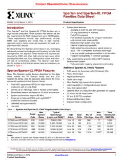
6 SelectIO HR I/O (GTP Transceivers)CPG23610 x (2)106 (2)106 (2)CPG23810 x (2)112 (2)CSG32415 x (0)210 (0)210 (0)210 (0)210 (0)CSG32515 x (2)150 (4)150 (4)150 (4)150 (4)FTG25617 x (0)170 (0)170 (0)170 (0)170 (0)SBG48419 x (4)FootprintCompatibleFGG484(5)23 x (4)250 (4)250 (4)285 (4)285 (4)FBG484(5)23 x (4)FootprintCompatibleFGG676(6)27 x (8)300 (8)FBG676(6)27 x (8)FFG115635 x (16)Page 5 Spartan-7 with the same last letter and number sequence, , A484, are footprint compatible with all other Spartan-7 devices with the same sequence. The footprint compatible devices within this Family are outlined. I/O Optimization at the Lowest Cost andHighest Performance-per-Watt( , )Part NumberXC7S6XC7S15XC7S25XC7S50 XC7S75XC7S100 Logic ResourcesLogic Cells6,00012,80023,36052,16076,800102,40 0 Slices9382,0003,6508,15012,00016,000 CLB Flip-Flops7,50016,00029,20065,20096,0001 28,000 Memory ResourcesMax.
7 Distributed RAM (Kb)701503136008321,100 Block RAM/FIFO w/ ECC (36 Kb each)510457590120 Total Block RAM (Kb)1803601,6202,7003,2404,320 Clock ResourcesClock Mgmt Tiles (1 MMCM + 1 PLL)223588I/O ResourcesMax. Single-Ended I/O Pins100100150250400400 Max. Differential I/O Pairs484872120192192 Embedded Hard IP ResourcesDSP Slices102080120140160 Analog Mixed Signal (AMS) / XADC001111 Configuration AES / HMAC Blocks001111 Speed GradesCommercialTemp (C)-1,-2-1,-2-1,-2-1,-2-1,-2-1,-2 Industrial Temp (I)-1,-2,-1L-1,-2,-1L-1,-2,-1L-1,-2,-1L- 1,-2,-1L-1,-2,-1 LExpanded Temp (Q)-1-1-1-1-1-1 Package(1)Body Area (mm)Ball Pitch(mm)Available User I/O: SelectIO HR 6 Spartan-6 FPGAsSpartan -6 LX FPGAsI/O Optimization at the Lowest Cost ( , )Spartan-6 LXT FPGAsI/O Optimization at the Lowest-Cost with Serial Connectivity ( )Part NumberXC6 SLX4XC6 SLX9XC6 SLX16XC6 SLX25XC6 SLX45XC6 SLX75XC6 SLX100XC6 SLX150XC6 SLX25 TXC6 SLX45 TXC6 SLX75 TXC6 SLX100 TXC6 SLX150 TSlices(1)6001,4302,2783,7586,82211,6621 5,82223,0383,7586,82211,66215,82223,038 Logic Cells(2)3,8409,15214,57924,05143,66174,6 37101,261147,44324,05143,66174,637101,26 1147,443 CLB Flip-Flops4,80011,44018,22430,06454,5769 3,296126,576184,30430,06454,57693,296126 ,576184,304 Max.
8 Distributed RAM (Kb)75901362294016929761,355229401692976 1,355 Block RAM (18Kb each)1232325211617226826852116172268268 Total Block RAM (Kb)(3)2165765769362,0883,0964,8244,8249 362,0883,0964,8244,824 Clock Mgmt Tiles (CMT)(4)2222466624666 Max. Single-Ended I/O Pins132200232266358408480576250296348498 540 Max. Differential I/O Pairs66100116133179204240288125148174249 270 DSP48A1 Slices(5)8163238581321801803858132180180 Endpoint Block for PCIe 11111 Memory Controller Blocks0222244422444 GTP Low-Power Transceivers 24888 Commercial Speed Grade(10)-1L, -2, -3-1L, -2, -3, -3N-1L, -2, -3, -3N-1L, -2, -3, -3N-1L, -2, -3, -3N-1L, -2, -3, -3N-1L, -2, -3, -3N-1L, -2, -3, -3N-2, -3, -3N-2, -3, -3N-2, -3, -3N-2, -3, -3N-2, -3, -3 NIndustrial Speed Grade(10)-1L, -2, -3-1L, -2, -3, -3N-1L, -2, -3, -3N-1L, -2, -3, -3N-1L, -2, -3, -3N-1L, -2, -3, -3N-1L, -2, -3, -3N-1L, -2, -3, -3N-2, -3, -3N-2, -3, -3N-2, -3, -3N-2, -3, -3N-2, -3, -3 NConfiguration Memory (Mb) Area (mm)Ball Pitch(mm)Maximum User I/O.
9 SelectIO Interface Pins (GTP Transceivers)(6)CPG196(7)8 x (7)20 x (8)13 x x (2)190 (4)CSG484(9)19 x (4)292 (4)296 (4)296 (4)FT(G)25617 x (G)484(9)23 x (2)296 (4)268 (4)296 (4)296 (4)FG(G)67627 x (8)376 (8)396 (8)FG(G)90031 x (8)540 (8)Notes: slice contains four LUTs and eight FPGA logic cell ratings reflect the increased logic capacity offered by the 6-input LUT RAM are fundamentally 18Kb in size. Each block can also be used as two independent 9 Kb CMT contains two DCMs and one DSP48A1 slice contains an 18x18 multiplier, an adder, and an LX device pinouts are not compatible with the LXT device and TQG144 do not have memory controller support. -3N is not available for these has X8 memory controller support in the LX9 and LX16 devices.
10 There is no memory controller in the LX4 in the FG(G)484 and CSG484 packages have support for two memory with -3N speed grade do not support MCB 7 CoolRunner-II CPLDsHigh performance and ultra-lowpower consumption in asingle-chip, instant-on programmable device( )Part Number XC2C32 AXC2C64 AXC2C128XC2C256XC2C384XC2C512 LogicResourcesSystem Gates 7501,5003,0006,0009,00012,000 Macrocells3264128256384512 Product Terms Per Macrocell565656565656 ClockResourcesGlobal Clocks 333333 Product Term Clocks Per Function Block 161616161616I/O ResourcesMaximum I/O 3364100184240270 Input Voltage Compatible / / / Voltage Compatible / / / GradesMin. Pin-to-Pin Logic Delay (ns) Speed Grades (Fastest to Slowest) -4, -6-5, -7-6, -7-6, -7-7, -10-7, -10 Industrial Speed Grades (Fastest to Slowest) -6-7-7-7-10-7(1), -10 Package(3), (4)Area (mm)Maximum User I/OsQFN Packages (QF): Quad, flat, no-lead ( lead spacing)QFG32(4)5 x 521 QFG48(4)7 x 737 VQFP Packages (VQ): Very thin QFP (VQ44: lead spacing, VQ100: lead spacing)VQG4412 x 123333 VQG10016 x 16648080 Chip Scale Packages (CP): Wire-bond, chip-scale, BGA ( ball spacing)CPG566 x 63345 CPG1328 x 8100106 TQFP Packages (TQ): Thin QFP ( lead spacing)TQG10016 x 16 TQG14422 x 22100118118 PQFP Packages (PQ): Wire-bond, plastic, QFP ( mm lead spacing) x mm173173173 FBGA Packages (FT).
