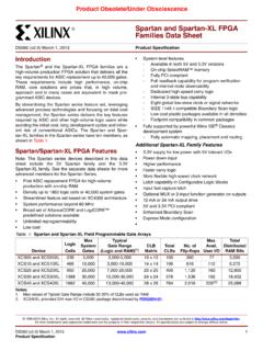
Transcription of Zynq-7000 SoC (Z-7030, Z-7035, Z-7045, and Z …
1 DS191 ( ) July 2, Specification1 Copyright 2012 2018 xilinx , Inc. xilinx , the xilinx logo, Zynq, Virtex, Artix, Kintex, Spartan, ISE, Vivado and other designated brands included herein are trademarks of xilinx in the United States and other countries. AMBA, AMBA Designer, ARM, Cortex-A9, CoreSight, Cortex, PrimeCell, ARM Powered, and ARM Connected Partner are trademarks of ARM Ltd. All other trademarks are the property of their respective Zynq -7000 SoCs are available in -3, -2, -2LI, -1, and -1LQ speed grades, with -3 having the highest performance. The -2LI devices operate at programmable logic (PL) VCCINT/VCCBRAM= and are screened for lower maximum static power. The speed specification of a -2LI device is the same as that of a -2 device. The -1LQ devices operate at the same voltage and speed as the -1Q devices and are screened for lower power. Zynq-7000 device DC and AC characteristics are specified in commercial, extended, industrial, and expanded (Q-temp) temperature ranges.
2 Except the operating temperature range or unless otherwise noted, all the DC and AC electrical parameters are the same for a particular speed grade (that is, the timing characteristics of a -1 speed grade industrial device are the same as for a -1 speed grade commercial device). However, only selected speed grades and/or devices are available in the commercial, extended, or industrial temperature supply voltage and junction temperature specifications are representative of worst-case conditions. The parameters included are common to popular designs and typical available device/package combinations are outlined in: Zynq-7000 SoC Overview (DS190) Defense-grade Zynq-7000Q SoC Overview (DS196) XA Zynq-7000 SoC Overview (DS188)This Zynq-7000 SoC data sheet, which covers the specifications for the XC7Z030, XA7Z030, XQ7Z030, XC7Z035, XC7Z045, XQ7Z045, XC7Z100, and XQ7Z100 complements the Zynq-7000 SoC documentation suite available on the xilinx website at Characteristics Zynq-7000 SoC(Z-7030, Z-7035, Z-7045, and Z-7100):DC and AC Switching CharacteristicsDS191 ( ) July 2, 2018 Product SpecificationTable 1.
3 Absolute Maximum Ratings(1)SymbolDescriptionMinMaxUnitsPr ocessing System (PS)VCCPINTPS internal logic supply voltage auxiliary supply voltage PLL supply DDR I/O supply (2)PS MIO I/O supply input reference voltage (2)(3)(4)(5)PS MIO I/O input voltage + DDR I/O input voltage + Logic (PL)VCCINTPL internal supply voltage supply voltage for the block RAM memories auxiliary supply voltage output drivers supply voltage for HR I/O banks output drivers supply voltage for HP I/O banks (4)Auxiliary supply voltage FeedbackZynq-7000 SoC (Z-7030, Z-7035, Z-7045, and Z-7100): DC and AC Switching CharacteristicsDS191 ( ) July 2, Specification2 VREFI nput reference voltage (3)(4)(5)I/O input voltage for HR I/O banks + input voltage for HP I/O banks + input voltage (when VCCO= ) for VREF and differential I/O standards except TMDS_33(6) VVCCBATTKey memory battery backup supply TransceiverVMGTAVCCA nalog supply voltage for the GTX transmitter and receiver circuits supply voltage for the GTX transmitter and receiver termination circuits analog Quad PLL (QPLL) voltage supply for the GTX transceivers transceiver reference clock absolute input voltage supply voltage for the resistor calibration circuit of the GTX transceiver column (RXP/RXN) and Transmitter (TXP/TXN)
4 Absolute input voltage input current for receiver input pins DC coupled RX termination = floating 14mAIDCIN-MGTAVTTDC input current for receiver input pins DC coupled RX termination = VMGTAVTT 12mAIDCIN-GNDDC input current for receiver input pins DC coupled RX termination = GND output current for transmitter pins DC coupled RX termination = floating 14mAIDCOUT-MGTAVTTDC output current for transmitter pins DC coupled RX termination = VMGTAVTT 12mAXADCVCCADCXADC supply relative to GNDADC reference input relative to GNDADC temperature (ambient) 65150 CTSOLM aximum soldering temperature for Pb/Sn component bodies(7) +220 CMaximum soldering temperature for Pb-free component bodies(7) +260 CTjMaximum junction temperature(7) +125 CNotes: beyond those listed under Absolute Maximum Ratings might cause permanent damage to the device. These are stress ratings only, and functional operation of the device at these or any other conditions beyond those listed under Operating Conditions is not implied.
5 Exposure to Absolute Maximum Ratings conditions for extended periods of time might affect device to both MIO supply banks VCCO_MIO0 and lower absolute voltage specification always I/O operation, refer to the 7 Series FPGAs SelectIO Resources User Guide (UG471) or the Zynq-7000 SoC Technical Reference Manual (UG585). maximum limit applies to DC signals. For maximum undershoot and overshoot AC specifications, see Table 4 and Table Table 12 for TMDS_33 soldering guidelines and thermal considerations, see the Zynq-7000 SoC Packaging and Pinout Specification (UG865).Table 1:Absolute Maximum Ratings(1) (Cont d)SymbolDescriptionMinMaxUnitsSend FeedbackZynq-7000 SoC (Z-7030, Z-7035, Z-7045, and Z-7100): DC and AC Switching CharacteristicsDS191 ( ) July 2, Specification3 Table 2:Recommended Operating Conditions(1)(2)SymbolDescriptionMinTypM axUnitsPSVCCPINT(3)PS internal logic supply auxiliary supply PLL supply DDR supply (4)PS supply voltage for MIO (5)PS DDR and MIO I/O input voltage VCCO_DDR+ VCCO_MIO+ (6)PL internal supply -2LI ( ) internal supply (6)PL block RAM supply -2LI ( ) block RAM supply auxiliary supply (7)(8)PL supply voltage for HR I/O supply voltage for HP I/O (9)PL auxiliary supply voltage when set to auxiliary supply voltage when set to (5)I/O input voltage VCCO+ input voltage (when VCCO= ) for VREF and differential I/O standards except TMDS_33(10) (11)Maximum current through any (PS or PL) pin in a powered or unpowered bank when forward biasing the clamp diode 10 mAVCCBATT(12)Battery TransceiverVMGTAVCC(13)Analog supply voltage for the GTX transceiver QPLL frequency range GHz(14)(15) supply voltage for the GTX transceiver QPLL frequency range > (13)
6 Analog supply voltage for the GTX transmitter and receiver termination (13)Auxiliary analog QPLL voltage supply for the (13)Analog supply voltage for the resistor calibration circuit of the GTX transceiver supply relative to supplied reference FeedbackZynq-7000 SoC (Z-7030, Z-7035, Z-7045, and Z-7100): DC and AC Switching CharacteristicsDS191 ( ) July 2, Specification4 TemperatureTjJunction temperature operating range for commercial (C) temperature devices0 85 CJunction temperature operating range for extended (E) temperature devices0 100 CJunction temperature operating range for industrial (I) temperature devices 40 100 CJunction temperature operating range for expanded (Q) temperature devices 40 125 CNotes: voltages are relative to ground. The PL and PS share a common the design of the power distribution system consult the Zynq-7000 SoC PCB Design Guide (UG933). the processor cores operate FCPU_6X4X_621_MAX at 1 GHz (-3E speed grade) or when the DDR interface operates at 1333 Mb/s, the VCCPINT minimum is and the VCCPINT maximum is to both MIO supply banks VCCO_MIO0 and lower absolute voltage specification always and VCCBRAM should be connected to the same data is retained even if VCCO drops to VCCO of , , , , (HR I/O only), and (HR I/O only) at 5%.
7 More information, refer to the VCCAUX_IO section of the 7 Series FPGAs SelectIO Resources User Guide (UG471) or the Zynq-7000 SoC Technical Reference Manual (UG585).10. See Table 12 for TMDS_33 A total of 200 mA per PS or PL bank should not be VCCBATT is required only when using bitstream encryption. If battery is not used, connect VCCBATT to either ground or Each voltage listed requires the filter circuit described in the 7 Series FPGAs GTX/GTH Transceivers User Guide (UG476).14. For data rates Gb/s, VMGTAVCC should be 3% for lower power For lower power consumption, VMGTAVCC should be 3% over the entire CPLL frequency 2:Recommended Operating Conditions(1)(2) (Cont d)SymbolDescriptionMinTypMaxUnitsSend FeedbackZynq-7000 SoC (Z-7030, Z-7035, Z-7045, and Z-7100): DC and AC Switching CharacteristicsDS191 ( ) July 2, Specification5 Table 3:DC Characteristics Over Recommended Operating ConditionsSymbolDescriptionMinTyp(1)MaxU nitsVDRINTData retention VCCINT voltage (below which configuration data might be lost) VVDRIData retention VCCAUX voltage (below which configuration data might be lost) VIREFPS_DDR_VREF 0/1, PS_MIO_VREF, and VREF leakage current per pin 15 AILI nput or output leakage current per pin (sample-tested) 15 ACIN(2)PL die input capacitance at the pad 8pFCPIN(2)PS die input capacitance at the pad 8pFIRPUPad pull-up (when selected) @ VIN=0V, VCCO= 330 APad pull-up (when selected) @ VIN=0V, VCCO= 250 APad pull-up (when selected) @ VIN=0V, VCCO= 220 APad pull-up (when selected) @ VIN=0V, VCCO= 150 APad pull-up (when selected) @ VIN=0V, VCCO= 120 AIRPDPad pull-down (when selected) @ VIN= 330 APad pull-down (when selected) @ VIN= 180 AICCADCA nalog supply current, analog circuits in powered up state 25mAIBATT(3)Battery supply current 150nARIN_TERM(4)
8 Thevenin equivalent resistance of programmable input termination to VCCO/2 (UNTUNED_SPLIT_40)284055 Thevenin equivalent resistance of programmable input termination to VCCO/2 (UNTUNED_SPLIT_50)355065 Thevenin equivalent resistance of programmable input termination to VCCO/2 (UNTUNED_SPLIT_60)446083 nTemperature diode ideality factor rTemperature diode series resistance 2 Notes: values are specified at nominal voltage, 25 measurement represents the die capacitance at the pad, not including the value specified for worst case process at 25 resistance to a VCCO/2 FeedbackZynq-7000 SoC (Z-7030, Z-7035, Z-7045, and Z-7100): DC and AC Switching CharacteristicsDS191 ( ) July 2, Specification6 Table 4:VIN Maximum Allowed AC Voltage Overshoot and Undershoot for PS I/O and PL HR I/O Banks(1)(2)AC Voltage Overshoot% of UI @ 40 C to 125 CAC Voltage Undershoot% of UI @ 40 C to 125 CVCCO+ + + + + + + + + : total of 200 mA per bank should not be peak voltage of the overshoot or undershoot, and the duration above VCCO+ or below GND , must not exceed the values in this 5:VIN Maximum Allowed AC Voltage Overshoot and Undershoot for PL HP I/O Banks(1)(2)AC Voltage Overshoot% of UI at 40 C to 125 CAC Voltage Undershoot% of UI at 40 C to 125 CVCCO+ + (3) (3)VCCO+ (3) (3)VCCO+ (3)VCCO+ (3)VCCO+ (3)VCCO+ + + : total of 200 mA per bank should not be peak voltage of the overshoot or undershoot, and the duration above VCCO+ or below GND , must not exceed the values in this UI lasting less than 20 FeedbackZynq-7000 SoC (Z-7030, Z-7035, Z-7045, and Z-7100): DC and AC Switching CharacteristicsDS191 ( ) July 2, Specification7 Table 6.
9 Typical Quiescent Supply CurrentSymbolDescriptionDeviceSpeed GradeUnits-3E-2E-2I-2LI-1C-1I-1Q-1 LQICCPINTQPS quiescent VCCPINT supply currentXC7Z03012212212279122122N/AN/AmAX C7Z03512212212279122122N/AN/AmAXC7Z04512 212212279122122N/AN/AmAXC7Z100N/AN/A1227 9N/A122N/AN/AmAXA7Z030N/AN/AN/AN/AN/A122 122N/AmAXQ7Z030N/AN/A12279N/A122122N/AmA XQ7Z045N/AN/A12279N/A122122122mAXQ7Z100N /AN/A12279N/A122N/AN/AmAICCPAUXQPS quiescent VCCPAUX supply currentXC7Z030131313111313N/AN/AmAXC7Z03 5131313111313N/AN/AmAXC7Z045131313111313 N/AN/AmAXC7Z100N/AN/A1311N/A13N/AN/AmAXA 7Z030N/AN/AN/AN/AN/A1313N/AmAXQ7Z030N/AN /A1311N/A1313N/AmAXQ7Z045N/AN/A1311N/A13 1313mAXQ7Z100N/AN/A1311N/A13N/AN/AmAICCD DRQPS quiescent VCCO_DDR supply currentXC7Z030444444N/AN/AmAXC7Z03544444 4N/AN/AmAXC7Z045444444N/AN/AmAXC7Z100N/A N/A44N/A4N/AN/AmAXA7Z030N/AN/AN/AN/AN/A4 4N/AmAXQ7Z030N/AN/A44N/A44N/AmAXQ7Z045N/ AN/A44N/A444mAXQ7Z100N/AN/A44N/A4N/AN/Am AICCINTQPL quiescent VCCINT supply currentXC7Z030246246246141246246N/AN/AmA XC7Z035611611611351611611N/AN/AmAXC7Z045 611611611351611611N/AN/AmAXC7Z100N/AN/A7 95457N/A795N/AN/AmAXA7Z030N/AN/AN/AN/AN/ A246246N/AmAXQ7Z030N/AN/A246141N/A246246 N/AmAXQ7Z045N/AN/A611351N/A611611611mAXQ 7Z100N/AN/A795457N/A795N/AN/AmASend FeedbackZynq-7000 SoC (Z-7030, Z-7035, Z-7045, and Z-7100).
10 DC and AC Switching CharacteristicsDS191 ( ) July 2, Specification8 ICCAUXQPL quiescent VCCAUX supply currentXC7Z030565656505656N/AN/AmAXC7Z03 5131131131117131131N/AN/AmAXC7Z045131131 131117131131N/AN/AmAXC7Z100N/AN/A165148N /A165N/AN/AmAXA7Z030N/AN/AN/AN/AN/A5656N /AmAXQ7Z030N/AN/A5650N/A5656N/AmAXQ7Z045 N/AN/A131117N/A131131131mAXQ7Z100N/AN/A1 65148N/A165N/AN/AmAICCAUX_IOQPL quiescent VCCAUX_IO supply currentXC7Z030222122N/AN/AmAXC7Z03522212 2N/AN/AmAXC7Z045222122N/AN/AmAXC7Z100N/A N/A21N/A2N/AN/AmAXA7Z030N/AN/AN/AN/AN/A2 2N/AmAXQ7Z030N/AN/A21N/A22N/AmAXQ7Z045N/ AN/A21N/A222mAXQ7Z100N/AN/A21N/A2N/AN/Am AICCOQPL quiescent VCCO supply currentXC7Z030444444N/AN/AmAXC7Z03544444 4N/AN/AmAXC7Z045444444N/AN/AmAXC7Z100N/A N/A44N/A4N/AN/AmAXA7Z030N/AN/AN/AN/AN/A4 4N/AmAXQ7Z030N/AN/A44N/A44N/AmAXQ7Z045N/ AN/A44N/A444mAXQ7Z100N/AN/A44N/A4N/AN/Am AICCBRAMQPL quiescent VCCBRAM supply currentXC7Z030111111 6 1111N/AN/AmAXC7Z035232323132323N/AN/AmAX C7Z045232323132323N/AN/AmAXC7Z100N/AN/A3 319N/A33N/AN/AmAXA7Z030N/AN/AN/AN/AN/A11 11N/AmAXQ7Z030N/AN/A116N/A1111N/AmAXQ7Z0 45N/AN/A2313N/A232323mAXQ7Z100N/AN/A3319 N/A33N/AN/AmANotes: values are specified at nominal voltage, 85 C junction temperatures (Tj) with single-ended SelectIO values are for blank configured devices with no output current loads, no active input pull-up resistors, all I/O pins are 3-state and the xilinx Power Estimator (XPE) spreadsheet tool (download at ) to estimate static power consumption for conditions other than those 6:Typical Quiescent Supply Current (Cont d)SymbolDescriptionDeviceSpeed GradeUnits-3E-2E-2I-2LI-1C-1I-1Q-1 LQSend FeedbackZynq-7000 SoC (Z-7030, Z-7035, Z-7045, and Z-7100).
