Transcription of Zynq UltraScale+ MPSoC Data Sheet: Overview (DS891)
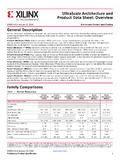
1 zynq ultrascale + MPSoC Data Sheet: Overview DS891 ( ) October 2, 2019 Product Specification General Description The zynq ultrascale + MPSoC family is based on the xilinx ultrascale MPSoC architecture. This family of products integrates a feature-rich 64-bit quad-core or dual-core Arm Cortex -A53 and dual-core Arm Cortex-R5 based processing system (PS) and xilinx programmable logic (PL) ultrascale architecture in a single device. Also included are on-chip memory, multiport external memory interfaces, and a rich set of peripheral connectivity interfaces. Processing System (PS).
2 Arm Cortex-A53 Based Application Dual-core Arm Cortex-R5 Based Processing Unit (APU) Real-Time Processing Unit (RPU). Quad-core or dual-core CPU frequency: Up to 600 MHz CPU frequency: Up to Armv7-R Architecture Extendable cache coherency o A32/T32 instruction set Armv8-A Architecture Single/double precision Floating Point Unit (FPU). o 64-bit or 32-bit operating modes CoreSight and Embedded Trace Macrocell o TrustZone security (ETM). o A64 instruction set in 64-bit mode, Lock-step or independent operation A32/T32 instruction set in 32-bit mode Timer and Interrupts: NEON Advanced SIMD media-processing engine o One watchdog timer Single/double precision Floating Point Unit (FPU) o Two triple-timer counters CoreSight and Embedded Trace Macrocell (ETM) Caches and Tightly Coupled Memories (TCMs).
3 Accelerator Coherency Port (ACP) o 32KB Level 1, 4-way set-associative AXI Coherency Extension (ACE) instruction and data cache with ECC. Power island gating for each processor core (independent for each CPU). Timer and Interrupts o 128KB TCM with ECC (independent for each CPU) that can be combined to become 256KB. o Arm Generic timers support in lockstep mode o Two system level triple-timer counters o One watchdog timer On-Chip Memory o One global system timer Caches 256KB on-chip RAM (OCM) in PS with ECC. o 32KB Level 1, 2-way set-associative Up to 36Mb on-chip RAM (UltraRAM) with ECC in instruction cache with parity (independent for PL.)
4 Each CPU) Up to 35Mb on-chip RAM (block RAM) with ECC. o 32KB Level 1, 4-way set-associative data in PL. cache with ECC (independent for each CPU) Up to 11Mb on-chip RAM (distributed RAM) in PL. o 1MB 16-way set-associative Level 2 cache with ECC (shared between the CPUs). Copyright 2015 2019 xilinx , Inc. xilinx , the xilinx logo, Alveo, Artix, Kintex, Spartan, Versal, Virtex, Vivado, zynq , and other designated brands included herein are trademarks of xilinx in the United States and other countries. AMBA, AMBA Designer, Arm, Arm1176JZ-S, CoreSight, Cortex, PrimeCell, Mali, and MPCore are trademarks of Arm in the EU and other countries.
5 PCI, PCIe, and PCI Express are trademarks of PCI-SIG and are used under license. All other trademarks are the property of their respective owners. DS891 ( ) October 2, 2019 Product Specification 1. zynq ultrascale + MPSoC Data Sheet: Overview Arm Mali-400 Based GPU Four 10/100/1000 tri-speed Ethernet MAC. peripherals with IEEE Std and IEEE Std 1588. Supports OpenGL ES and revision support Supports OpenVG o Scatter-gather DMA capability GPU frequency: Up to 667 MHz o Recognition of IEEE Std 1588 PTP frames Single Geometry Processor, Two Pixel Processors o GMII, RGMII, and SGMII interfaces Pixel Fill Rate: 2 Mpixels/sec/MHz o Jumbo frames Triangle Rate.
6 Mtriangles/sec/MHz Two USB Device, Host, or OTG peripherals, 64KB L2 Cache each supporting up to 12 endpoints Power island gating o USB compliant device IP core o Super-speed, high- speed, full-speed, and External Memory Interfaces low-speed modes Multi-protocol dynamic memory controller o Intel XHCI- compliant USB host 32-bit or 64-bit interfaces to DDR4, DDR3, Two full CAN CAN bus interfaces DDR3L, or LPDDR3 memories, and 32-bit o CAN and CAN and ISO 118981-1. interface to LPDDR4 memory standard compliant ECC support in 64-bit and 32-bit modes Two SD/SDIO compliant Up to 32GB of address space using single or dual controllers rank of 8-, 16-, or 32-bit-wide memories Two full-duplex SPI ports with three peripheral Static memory interfaces chip selects o Managed NAND flash support Two high-speed UARTs (up to 1Mb/s).
7 O NAND flash with 24-bit ECC Two master and slave I2C interfaces o 1-bit SPI, 2-bit SPI, 4-bit SPI (Quad-SPI), or Up to 78 flexible multiplexed I/O (MIO) (up to two Quad-SPI (8-bit) serial NOR flash three banks of 26 I/Os) for peripheral pin assignment 8-Channel DMA Controller Up to 96 EMIOs (up to three banks of 32 I/Os). connected to the PL. Two DMA controllers of 8-channels each Memory-to-memory, memory-to-peripheral, Interconnect peripheral-to-memory, and scatter-gather High-bandwidth connectivity within PS. transaction support and between PS and PL. Serial Transceivers Arm AMBA AXI4-based QoS support for latency and bandwidth control Four dedicated PS-GTR receivers and Cache Coherent Interconnect (CCI).
8 Transmitters supports up to data rates o Supports SGMII tri-speed Ethernet, PCI System Memory Management Express Gen2, Serial-ATA (SATA), , System Memory Management Unit (SMMU). and DisplayPort xilinx Memory Protection Unit (XMPU). Dedicated I/O Peripherals and Platform Management Unit Interfaces Power gates PS peripherals, power islands, and PCI Express Compliant with PCIe base power domains specification Clock gates PS peripheral user firmware option o Root complex and End Point configurations o x1, x2, and x4 at Gen1 or Gen2 rates Configuration and Security Unit SATA Host Boots PS and configures PL.
9 O , , and data rates as defined by Supports secure and non-secure boot modes SATA Specification, revision o Supports up to two channels System Monitor in PS. DisplayPort Controller On-chip voltage and temperature sensing o Up to rate o Up to two TX lanes (no RX support). DS891 ( ) October 2, 2019 Product Specification 2. zynq ultrascale + MPSoC Data Sheet: Overview Programmable Logic (PL). Configurable Logic Blocks (CLB) PCI Express Look-up tables (LUT) Supports Root complex and End Point Flip-flops configurations Cascadable adders Supports up to Gen3 speeds Up to five integrated blocks in select devices 36Kb Block RAM.
10 True dual-port 100G Ethernet MAC/PCS. Up to 72 bits wide IEEE Std compliant Configurable as dual 18Kb CAUI-10 (10x ) or CAUI-4 (4x ). UltraRAM RSFEC (IEEE Std ) in CAUI-4 configuration Up to four integrated blocks in select devices 288Kb dual-port 72 bits wide Interlaken Error checking and correction Interlaken spec compliant DSP Blocks 64/67 encoding 12 x or 6 x 25Gb/s 27 x 18 signed multiply Up to four integrated blocks in select devices 48-bit adder/accumulator 27-bit pre-adder Video Encoder/Decoder (VCU). Programmable I/O Blocks Available in EV devices Accessible from either PS or PL.