Epitaxial Silicon
Found 9 free book(s)
SS8550 - PNP Epitaxial Silicon Transistor
www.onsemi.comPNP Epitaxial Silicon Transistor SS8550 Features • 2 W Output Amplifier of Portable Radios in Class B Push−Pull Operation • Complementary to SS8050 • Collector Current: IC = 1.5 A • These Devices are Pb−Free, Halogen Free/BFR Free and are RoHS Compliant ABSOLUTE MAXIMUM RATINGS (TA = 25°C unless otherwise noted) Parameter Symbol ...
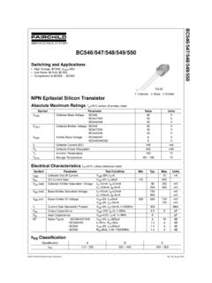
BC546/547/548/549/550 NPN Epitaxial Silicon Transistor
www.sparkfun.comNPN Epitaxial Silicon Transistor Absolute Maximum Ratings Ta=25°C unless otherwise noted Electrical Characteristics Ta=25°C unless otherwise noted hFE Classification Symbol Parameter Value Units VCBO Collector-Base Voltage : BC546 : BC547/550: BC548/549 80 50 30 V V V VCEO Collector-Emitter Voltage : BC546 : BC547/550: BC548/549 65 45 30 V V V
UTC - NKC Electronics
media.nkcelectronics.comutc s8050 npn epitaxial silicon transistor utc unisonic technologies co., ltd.1 qw-r201-013,a low voltage high current small signal npn transistor description the utc s8050 is …

ON Semiconductor Is Now
www.onsemi.comNPN Epitaxial Silicon Transistor Absolute Maximum Ratings Ta=25°C unless otherwise noted Electrical Characteristics Ta=25°C unless otherwise noted * Pulse Test: Pulse Width≤300µs, Duty Cycle≤2% Symbol Parameter Value Units VCBO Collector-Base Voltage 60 V VCEO Collector-Emitter Voltage 30 V VEBO Emitter-Base Voltage 5 V IC Collector ...

Silicon Wafer Processing - National Chiao Tung University
jupiter.math.nctu.edu.twGrowth of Epitaxial Silicon This step is done to provide a good clean surface for later processing. If a layer of Silicon is grown onto the top of the wafer using chemical methods then that layer is of a much better quality then the slightly damaged or unclean layer of silicon in the wafer. The epitaxial layer is where the actual processing will be
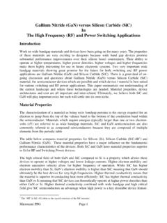
Gallium Nitride (GaN) versus Silicon Carbide (SiC)
www.richardsonrfpd.comswitching and RF power applications require an epitaxial layer of either SiC or GaN to be grown or deposited on a substrate composed of either the same (homoepitaxy) or a different (heteroepitaxy) material. Homoepitaxial SiC devices are fabricated in a way that is analogous to silicon in that a SiC epi

2SC1815 2SC1815-O 2SC1815-Y 2SC1815-GR 2SC1815-BL ...
www.mouser.comSILICON NPN TRANSISTORS DESCRIPTION: The CENTRAL SEMICONDUCTOR 2SC1815 Series are silicon NPN transistors, manufactured by the epitaxial planar process, designed for general purpose amplifier applications. MARKING: FULL PART NUMBER MAXIMUM RATINGS: (TA=25°C unless otherwise noted) SYMBOL UNITS Collector-Base Voltage VCBO 60 V

Silicon Carbide and Nitride Materials Catalog
assets.wolfspeed.comEpitaxial Layers SiC and GaN materials enable faster, smaller, lighter and more powerful electronic systems. Wolfspeed is committed ... Silicon Face CMP 6 = Double-side Polish, Carbon Face CMP C1 = 350 µm Thickness N = 500 µm Thickness w/ notch This character only applicable to 150 mm wafers. 0 = On-Axis

Silicon Basics --General Overview. - Columbia University
www1.columbia.eduSurface properties of silicon. Surface structure and properties are critically important in semiconductor processing! • Deposition and etch properties are highly dependent upon surface structure and chemistry. • Epitaxial growth relies on surface structure. • Junction properties can be influenced. Much of this section adapted from