Search results with tag "Silicon"

RCA-1 Silicon Wafer Cleaning - INRF
www.inrf.uci.eduoxidative desorption and complexing with H2O2-NH4OH-H2O (RCA1). A second RCA-2 clean (SC-2) is often used H2O2-HCI-H2O to further clean the surface. RCA-1 clean is used to remove organic residues from silicon wafers. In the process, it oxidizes the silicon and leaves a thin oxide on the surface of the wafer, which should be removed
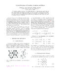
Crystal Structure of Graphite, Graphene and Silicon
community.wvu.eduMar 13, 2009 · tor material, silicon (Si) is featured in Figure 3. Silicon forms a diamond cubic crystal structure with a lattice spacing of 5.42˚A. This crystal structure corresponds to a face-centered cubic Bravais lattice whose unit-cell basis contains 8 atoms located at vector positions, d0 =~0 d4 = a 4 (1,3,3) d1 = a 4 (1,1,1) d5 = a 4 (2,2,0) d2 = a 4 ...

High Voltage Silicon Carbide Power Devices
www.arpa-e.energy.govHigh Voltage Silicon Carbide Power Devices Creating Technology That Creates Solutions John W. Palmour Cree, Inc. 4600 Silicon Drive Durham, NC 27703; USA Tel:: 919-313-5646 Email: john_palmour@cree.com. SiC MOSFETs and Schottky Diodes show Zero Q rr 2 4 6 8 10 Reduced Losses Using SiC JBS Diode

BCP53 Series PNP Silicon Epitaxial Transistors
www.onsemi.comPNP Silicon Epitaxial Transistors This PNP Silicon Epitaxial transistor is designed for use in audio amplifier applications. The device is housed in the SOT−223 package which is designed for medium power surface mount applications. • High Current • NPN Complement is BCP56 • The SOT−223 Package can be soldered using wave or reflow.
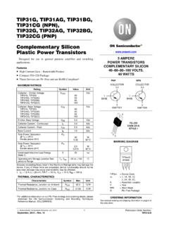
TIP31A - Complementary Silicon Plastic Power Transistors
www.onsemi.comComplementary Silicon Plastic Power Transistors Designed for use in general purpose amplifier and switching applications. Features • High Current Gain − Bandwidth Product • Compact TO−220 Package • These Devices are Pb−Free and are RoHS Compliant* MAXIMUM RATINGS Rating Symbol Value Unit Collector − Emitter Voltage TIP31G, TIP32G ...

SS8550 - PNP Epitaxial Silicon Transistor - ON Semiconductor
www.onsemi.comPNP Epitaxial Silicon Transistor SS8550 Features • 2 W Output Amplifier of Portable Radios in Class B Push−Pull Operation • Complementary to SS8050 • Collector Current: IC = 1.5 A • These Devices are Pb−Free, Halogen Free/BFR Free and are RoHS Compliant ABSOLUTE MAXIMUM RATINGS (TA = 25°C unless otherwise noted) Parameter Symbol ...

2SC1815 2SC1815-O 2SC1815-Y 2SC1815-GR 2SC1815-BL ...
www.mouser.comSILICON NPN TRANSISTORS DESCRIPTION: The CENTRAL SEMICONDUCTOR 2SC1815 Series are silicon NPN transistors, manufactured by the epitaxial planar process, designed for general purpose amplifier applications. MARKING: FULL PART NUMBER MAXIMUM RATINGS: (TA=25°C unless otherwise noted) SYMBOL UNITS Collector-Base Voltage VCBO 60 V

Please use this setup by N1RWY to start with (I've ...
winlink.org• Silicon Labs Dual CP210x USB to UART Bridge: Enhanced COM Port (COM 4) (<–OR SOME OTHER NUMBER) • Silicon Labs Dual CP210x USB to UART Bridge: Standard COM Port (COM 5) (<–OR SOME OTHER NUMBER) Again, your new ports might be numbered 3 and 4, or 6 and 7, or some other combination. The key is

Cleaning Procedures for Silicon Wafers
www.inrf.uci.eduCleaning Procedures for Silicon Wafers INRF application note Process name: SOLVENTCLEAN + RCA01 + HFDIP . W. Kern and J. Vossen, Thin Film Processes, Academic Press: New York, 1978, Ch V-1 . W. Kern and Ed., Handbook of Semiconductor Cleaning Technology, Noyes Publishing: Park Ridge, NJ, 1993 Ch 1. Checklist

400 W+ 0/+5 W 20.8 %
static.trinasolar.comBACKSHEET MONOCRYSTALLINE MODULE 400 W+ MAXIMUM POWER OUTPUT POSITIVE POWER TOLERANCE MAXIMUM EFFICIENCY Outstanding Visual Appearance ... Silicon Sealant Frame 30 33 B-B 15.4 Laminate Silicon Sealant Nameplate A A B B Junction Box 1048 1100 6-Φ4.3 Grounding Hole 12-Drain Hole Installing Hole Current (A) Voltage (V) 1.0 2.0 3.0 …

SS8050 - NPN Epitaxial Silicon Transistor
www.mouser.comNPN Epitaxial Silicon Transistor Features • 2 W Output Amplifier of Portable Radios in Class B Push-pull Operation. • Complimentary to SS8550 • Collector Current: IC = 1.5 A Ordering Information Absolute Maximum Ratings Stresses exceeding the absolute maximum ratings may damage the device. The device may not function or be opera-

BC550 - NPN Epitaxial Silicon Transistor
www.onsemi.comNPN Epitaxial Silicon Transistor BC546 / BC547 / BC548 / BC549 / BC550 Features • Switching and Amplifier • High−Voltage: BC546, VCEO = 65 V • Low−Noise: BC549, BC550 • Complement to BC556, BC557, BC558, BC559, and BC560 • These are Pb−Free Devices ABSOLUTE MAXIMUM RATINGS Parameter Symbol Value Unit Collector−Base Voltage ...

CVD diamond handbook - United States
e6cvd.comsilicon 14 28.085 P phosphorus 15 30.973 High-pressure, high-temperature synthetic diamond is usually nitrogen doped, giving it a distinctive yellow hue. Carbon’s position as a group IV element above silicon in the periodic table. 4 Physical properties ... diamond wafers can be fabricated 120 mm in diameter, with thermal and infrared ...
AN249: Human Interface Device Tutorial - Silicon Labs
www.silabs.comSilicon Laboratories’ USBXpress, which includes a set of custom drivers, firmware routines, and host routines that enable USB communication. HID-class devices simplify USB communication one step further by using a standardized, flexible driver that comes pre-installed with all commonly-used operating systems. Benefits of developing with HID ...

Answers to Worksheet Writing Equations
www.mrsterrylhs.weebly.comh) Silicon dioxide solid plus aqueous hydrofluoric acid (HF) yields solid silicon tetrafluoride plus liquid water. SiO2(s) + HF(aq) SiF4(s) + H2O(l) i) Aqueous sodium hydroxide and carbon dioxide gas yields sodium carbonate solution and liquid water. NaOH(aq) + CO2(g) Na2CO3(aq) + H2O(l)

Solar Energy -- Energy from the Sun - Lehigh University
ei.lehigh.educommonly called a solar cell or PV, is the technology used to convert solar energy directly into electrical power. A photovoltaic cell is a nonmechanical device usually made from silicon alloys. Sunlight is composed of photons, or particles of solar energy. These photons contain various amounts of energy corresponding to the different

AMBA Specification - University of Waterloo
student.cs.uwaterloo.caIf you have any comments on this document, please send email to errata@arm.com giving: • the document title • the document number • the page number(s) to which your comments refer ... • to minimize the silicon infrastructure required to support efficient on-chip and off-chip communication for both operation and manufacturing test.
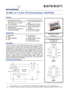
Si570/Si571 Data Sheet - Silicon Labs
www.skyworksinc.comJ 12 kHz to 20 MHz (OC-48) — 0.25 0.40 ps 50 kHz to 80 MHz (OC-192) — 0.26 0.37 Phase Jitter (RMS)1 for FOUT of 125 to 500 MHz J 12 kHz to 20 MHz (OC-48) — 0.36 0.50 ps 50 kHz to 80 MHz (OC-192)2 — 0.34 0.42 Phase Jitter (RMS) for FOUT of 10 to 160 MHz CMOS Output Only J 12 kHz to 20 MHz (OC-48)2 —0.62 — ps 50 kHz to 20 MHz2 —0.61 ...

1.EMITTER 2. BASE 3. COLLECT
atta.szlcsc.comNPN silicon epitaxial planar transistor for switching and Amplifier applications As complementary type, the PNP transistor 2N3906 is Recommended This transistor is also available in the SOT-23 case with the type designation MMBT3904 MAXIMUM RATINGS (T A=25℃ unless otherwise noted) SymbolParameterValue Units V CBO Collector-Base Voltage …
High Capacity Silicon-Graphene Anode for Li-Ion ... - NASA
www.nasa.gov• Flexible flake morphology provides better particle contact, • Helps to maintain the mechanical integrity of the electrode. 3. Utilize an existing, low-cost industrial manufacturing process • XG Sciences is already using the process for bulk production of xGnP® graphene nanoplatelets. 11
Totem-pole PFC reference design with SiC technology
www.st.comSilicon carbide MOSFET 650 V, 45 A TN3050H-12WY SCR Thyristor 30A 1200V 1200V 600V 600V 1200V STM32F334 VIPer26LD 97.5 % efficiency at full load Key Products: SCTW35N65G2V (SiC MOSFET) TN3050H-12GY (SCR Thyristor) STGAP2AS (Galvanic insulated gate driver) STM32F334 (32-bit MCU) VIPer26LD (converter for aux. PS)

Wide Bandgap Semiconductors: Pursuing the Promise
www1.eere.energy.govWide bandgap (WBG) semiconductor . materials allow power electronic components to be smaller, faster, more reliable, and more efficient than their silicon (Si)-based counterparts. These capabilities make it possible to reduce weight, volume, and life-cycle costs in a wide range of power applications. Harnessing these capabilities can lead

Pearson Edexcel International GCSE Chemistry
qualifications.pearson.comMay 17, 2018 · Silicon 14 31 P Phosphorus 15 32 S Sulfur 16 35.5 Cl Chlorine 17 40 Ar Argon 18 (a) (i) The elements in the Periodic Table are arranged in order of increasing (1) A atomic number B mass number C neutron number D relative atomic mass (ii) Identify the element that is in Period 3 and Group 5 of the Periodic Table. (1)

8-Ch/Dual 4-Ch High-Performance CMOS Analog Multiplexers
www.vishay.comDesigned in the 44 V silicon-gate CMOS process, the absolute maximum voltage rating is extended to 44 V. Additionally, single supply operation is also allowed. An epitaxial layer prevents latchup. For additional information please see Technical Article TA201. FEATURES • Low on-resistance - RDS(on): 100 • Low charge injection - Q: 20 pC

KSZ8041TL/FTL/MLL Data Sheet - Microchip Technology
ww1.microchip.comErrata An errata sheet, describing minor operational differences from the data sheet and recommended workarounds, may exist for cur-rent devices. As device/documentation issues become known to us, we will publish an errata sheet. The errata will specify the revision of silicon and revision of document to which it applies.

SMALL SIGNAL NPN TRANSISTOR - SparkFun Electronics
www.sparkfun.com2n3904 small signal npn transistor preliminary data silicon epitaxial planar npn transistor to-92 package suitable for through-hole pcb assembly the pnp complementary type is 2n3906 applications well suitable for tv and home appliance equipment

Dell EMC PowerEdge R650 Spec Sheet - Dell Technologies
www.delltechnologies.com• Silicon Root of Trust • System Lockdown (requires iDRAC9 Enterprise or Datacenter) • TPM 1.2/2.0 FIPS, CC-TCG certified, TCM 2.0 optional Embedded NIC 2 x 1 GbE LOM Network Options 1 x OCP 3.0 (x8 PCIe lanes) GPU Options Up to three 75 W single-width GPU Ports Front Ports • 1 x Dedicated iDRAC Direct micro-USB • 1 x USB 2.0 • 1 x VGA
AL 29-4C For Heating and Ventilating
www.atimetals.comSilicon Chromium Nickel Molybdenum . Nitrogen 0.02: Titanium+Columbium (Niobium) Iron Balance. 0.02 0.50 . 0.03 <0.01 . ... By using AL 29-4C heat exchangers, furnace manufacturers have benefited by being able to offer extended warranties in ... tool coatings such as titanium nitride have been helpful in extending tool life. Contact your ...

Vertical multi-stage centrifugal pumps
www.dp-pumps.comGeneral hazard sign according to ISO 7000-0434 ATTENTION Is used to introduce safety instructions whose non-observance may lead to damage to the product and its ... Silicon carbide Tungsten carbide Carbon graphite Resin impregnated Pressureless sintered CrNiMo-binder Resin impregnated, porous Seat ring Ca Ca SiC TuC Ce eSiC-Q7 A B Q1 U3 V Q7

Si7020-A20 - Silicon Labs
www.silabs.comSi7020-A20 6 Rev. 1.2 Figure 1. I2C Interface Timing Diagram Table 3. I2C Interface Specifications1 1.9 VDD 3.6 V; TA = –40 to +85 °C (G grade) or –40 to +125 °C (I/Y grade) unless otherwise noted. Parameter Symbol Test Condition Min Typ Max Unit Hysteresis VHYS High-to-low versus low-to- high transition 0.05 x VDD —— V SCLK Frequency2 f SCL — — 400 kHz
RA 253 MA Data Sheet - Rolled Alloys
www.rolledalloys.comRA 253 MA® Data Sheet Rolled Alloys 2 RA 253 MA® is a lean austenitic heat resistant alloy with high strength and outstanding oxidation resistance. RA 253 MA obtains its heat resistant properties by advanced control of microalloying additions. The use of rare earth metals in combination with silicon gives superior oxidation

Two Selectable Inputs, 12 LVPECL Outputs, SiGe Clock ...
www.analog.comthe Analog Devices, Inc., proprietary XFCB3 silicon germa-nium (SiGe) bipolar process. This device is designed for high speed applications requiring low jitter. The device has two selectable differential inputs via the IN_SEL control pin. Both inputs are equipped with center tapped, differential, 100 Ω on-chip termination resistors. The inputs

430-450W - Suntech Power
www.suntech-power.comSolar Cell Monocrystalline silicon 166 mm No. of Cells 144 (6 × 24) Dimensions 2096 × 1040 × 35 mm (82.5 × 40.9 × 1.4 inches) Weight 28.1 kgs (61.9 lbs.) Front \Back Glass 2.0 +2.0 mm (0.079 +0.079 inches) semi-tempered glass Frame Anodized aluminium alloy Junction Box IP68 rated Output Cables 4.0 mm2, (-) 350 mm and (+) 160 mm in length

SST26VF016B 2.5V/3.0V 16 Mbit Serial Quad I/O (SQI) Flash ...
ww1.microchip.comMay 14, 2019 · silicon and revision of document to which it applies. To determine if an errata sheet exists for a particular device, please check with one of the following: ... ual block to be controlled separately. In addition, the Write-Protection Lock-Down register prevents any
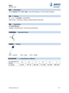
9013 - fsbrec.com
www.fsbrec.comTO-92 塑封封装 NPN 半导体三极管。Silicon NPN transistor in a TO-92 Plastic Package. PC 、IC 大, hFE 特性极好,与 9012 互补。 High P C and I C, excellent h FE linearity, complementary pair with 9012. 用于收音机推挽功放。 Amplifier of portable radios in class B push-pull operation.

APLYING VARIABLE SPEED DRIVES ON A ... - Rockwell …
literature.rockwellautomation.comSCR’s (Silicon Controlled Rectifier) or 6 diodes to create a full wave three phase bridge rectifier. For a three phase system, each phase creates 2 pulses resulting in what is called a 6 pulse rectified converter. The converter section is often refered to as the “front end”. The front end converts the 3 phase AC line to a DC voltage which ...

Latch-Up White Paper - Texas Instruments
www.ti.com(epitaxial silicon) layer. The EPI layer is doped appropriately for the best transistor performance (more lightly doped than the remaining lower portion of the substrate that is highly doped). The highly doped substrate directs majority carriers to ground and reflects minority carriers making the guard rings more effective (see Figure 3).

Material Safety Data Sheet Titanium Dioxide
www.titanium-dioxide.bizSilicon dioxide (CAS 7631-86-9) 3 Not classifiable as to carcinogenicity to humans. Titanium dioxide (CAS 13463-67-7) 2B Possibly carcinogenic to humans. Epidemiology None known. Mutagenicity No data available to indicate product or any components
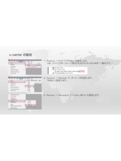
u-center の設定
www.n-survey.comSilicon Labs CP210x USB to UART Bridge (COM3) File Edit View Baudrate Location API Sensor API Player Receiver Tools Window Help Disconnect COM3 Network connection Ctrl-O Ctrl-3 Network connection NTRIP server/Caster... NTRIP Client... File Edit View Baudrate Location API sensor API Player Receiver Tools Window 1'200 2400 9600 19'200 38'400 57600 11
Virtual COM Port Install Manual
yaesu.com「Silicon Labs Dual CP210x USB to UART Bridge : Standard COM Port (COM**)」 ※(COM**)の部分の番号はパソコンの使用状況によって異なります。 USB接続に対応するトランシーバーまたはUSBインターフェースユニットSCU-17は、 Enhanced
RF Switches - QSL.net
www.qsl.net• The silicon switching diode is the most basic function of almost every electronic application. • Switching diodes are also used in high-speed rectifying applications, such as in radio receivers. Applications also include general-purpose switching and reverse

How to Configure the Yaesu FTDX101D for WSJT-X and JS8 ...
s873ba685ce580070.jimcontent.com6. The two Silicon Labs Dual CP2105 USB to UART Bridge port numbers need to be written down or remembered as you will need them for the WSJT-X configuration. 7. NOTE: they may be different on your PC depending on what other ports are in use etc. 8. Note in my case: a. COM3 is the Enhanced Port for my radio, and b. COM4 is the Standard Port for ...

VDS C3M0032120K I D R 32 mΩ
assets.wolfspeed.com1 C3M0032120K Rev. - 06-2019 C3M0032120K Silicon Carbide Power MOSFET C3M TM MOSFET Technology N-Channel Enhancement Mode Features • 3rd generation SiC MOSFET technology • Optimized package with separate driver source pin • 8mm of creepage distance between drain and source • High blocking voltage with low on-resistance • High-speed …

Cleaning procedures for glass substrates
www.inrf.uci.eduCleaning procedures for glass substrates INRF Application note ... Overview . Glass slides wafers are often cleaned by a solvent clean followed by a dionized water (DI) rinse, followed by a mild acid clean, DI rinse and blow dry. ... (do not exceed 55 deg C). Place silicon wafer in warn acetone bath for 10 minutes. Remove and place in methanol ...

Silicon Labs CP210x USB-to-UART - Digi-Key Electronics
www.digikey.comSilicon Labs CP210x USB-to-UART www.xilinx.com 4 UG1033 (v1.0) February 12, 2014 Silicon Labs CP210x USB-to-UART Installation Guide Overview Many Xilinx evaluation boards and some characterization boards are equipped with the Silicon Labs CP2103 USB-to-UART bridge integrated circuits. This guide explains how to

SILICON DIOXIDE, crystalline Safety Data Sheet SIS6964
www.gelest.comSILICON DIOXIDE, crystalline Safety Data Sheet 02/18/2015 EN (English US) SDS ID: SIS6964.0 2/6 First-aid measures after eye contact : Immediately flush eyes thoroughly with water for …
Similar queries
RCA-1 Silicon Wafer Cleaning, H2O2, Graphite, Silicon, Silicon Carbide Power Devices, PNP Silicon Epitaxial, PNP Silicon Epitaxial transistor, Complementary Silicon Plastic Power, Epitaxial silicon, Silicon NPN, Epitaxial, Silicon Labs, CP210x USB, Cleaning Procedures for Silicon Wafers, Cleaning, MONOCRYSTALLINE, BC550, NPN Epitaxial Silicon Transistor, Carbon, Wafers, SILICON DIOXIDE, Dioxide, Energy, Technology, Power, Device, AMBA, Errata, NPN silicon epitaxial, Transistor, High Capacity Silicon-Graphene Anode for, NASA, Particle, Silicon carbide MOSFET, SiC MOSFET, Wide bandgap, Semiconductor, SparkFun Electronics, Silicon epitaxial, Single, Using, Nitride, Hazard, Silicon Carbide, Carbide, Analog Devices, Monocrystalline silicon, Controlled, Plastic, Complementary, Rockwell, Rectifier, Phase bridge rectifier, Phase, Voltage, Texas Instruments, Silicon Labs CP210x USB to UART, Diode, USB to UART, MOSFET, Channel, Cleaning procedures, Digi-Key